Published:Zorapid.Ltd
Application Scope & Core Semiconductor Requirements
Typical Parts
- RF bias electrodes, plasma source components, heat sink bases, vacuum chamber conductive liners, electrical feedthrough pins, contact probes, ion implant electrodes, power bus bars, cooling manifold conductive inserts, wafer chuck conductive inserts, gas distribution conductive manifolds, grounding blocks
Non-Negotiable Semiconductor Core Criteria
- Ultra-high electrical conductivity: Minimize power loss, consistent RF/plasma performance
- Low outgassing (ASTM E595 / ASTM E1559): No volatile organics to contaminate wafers
- Ultra-low particulate / metallic ion contamination: Zero iron, chromium, nickel cross-contamination risk
- Vacuum compatibility (UHV 10⁻⁹ Torr+): Dense grain structure, no subsurface micro-pores
- ESD controlled production: Prevent static discharge damaging sensitive wafers
- Smooth, defect-free surfaces: Avoid plasma arcing, micro-field emission
- Thermal conductivity stability: Critical for RF heat dissipation & chuck temperature uniformity
- No residual cutting fluid, burrs, micro-swarf, embedded abrasive particles
Governing Standards
SEMI S2, SEMI F57, ASTM E595 outgassing, ISO 14644 cleanroom, ANSI/ESD S20.20, RoHS, IPC/JEDEC contamination specs, UHV helium leak testing standards
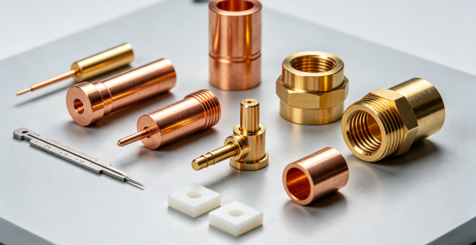
Key Copper / Brass Grades for Semiconductor Turning
Oxygen-Free High Conductivity Copper (OFHC C10100 / C10200) – Semiconductor Copper
- Core specs: <10 ppm oxygen, 101% IACS conductivity, high thermal transfer, low outgassing, UHV compatible
- Use case: RF electrodes, plasma bias plates, heat sinks, wafer chuck inserts, high-current bus bars
- Machining trait: Soft, ductile, prone to built-up edge (BUE), stringy chips, easy smearing on finished surfaces
- Risk: Uncontrolled turning leaves copper micro-swarf embedded into surfaces → plasma arcing & wafer metal contamination
C11000 Electrolytic Tough Pitch Copper (ETP)
- Lower cost, higher oxygen content, limited to non-plasma, non-UHV secondary conductive hardware only
- Not approved for etch/deposition chamber RF components (high oxygen = high outgassing + plasma sputtering risk)
Copper Alloys (Limited Semiconductor Use)
- CuZr / CuAg alloy: High strength + high conductivity for thin high-load electrode pins
- Avoid leaded copper, free-machining copper with sulfur additives – sulfur outgasses under plasma
Low-Lead Semiconductor Brass (C26000, C27000, Lead-Free C46400)
- Low zinc vapor pressure, low outgassing, moderate conductivity, superior machinability vs pure copper
- Use case: grounding blocks, low-current feedthroughs, non-plasma vacuum fittings, probe housings
- Critical rule: NO leaded brass (C36000) – lead sputters under plasma, causes fatal wafer contamination
- Limitation: Higher zinc content will sputter in high-energy plasma environments; not for direct plasma-facing surfaces
Material Receiving Validation Rules
- MTR mill certification for oxygen content, conductivity, impurity elemental analysis
- PMI XRF batch testing to screen iron, nickel, chromium, lead, sulfur contaminants
- Raw stock segregated fully from steel, stainless, aluminum to eliminate cross-contamination
- Pre-stress relieved bar stock to prevent post-turning dimensional drift in vacuum thermal cycles
Lathe & 5-Axis Turning Machine Specs
Cleanroom CNC Lathe / Turn-Mill Requirements
- Machine Enclosure: Fully sealed positive-pressure cabinet, HEPA/ULPA filtered recirculating air, ISO 7 / ISO 6 cleanroom integration
- Spindle: High-precision ceramic bearings, runout ≤0.002mm, balanced HSK tool holders, low-particulate sealed lubrication
- For micro conductive pins: Swiss type sliding headstock lathes (tiny feedthrough probe pins)
- Thermal Control: Machine base temperature stabilized ±0.1°C, linear glass scales, real-time thermal compensation
- ESD Design: Full machine frame conductive grounding, anti-static guideways, ESD-safe spindle covers, conductive chip conveyors
- Chip & Mist Extraction: Integrated ULPA filtered vacuum chip removal, closed mist collection system to stop airborne copper dust
- Lubrication: Food-grade / low-outgassing synthetic grease only; no mineral oil, heavy paraffin lubricants (high VOC outgassing risk)
- Controller: Locked validated turning recipes, MES batch traceability, cavity temperature monitoring for long conductive electrodes
Hybrid Turn-Mill 5-Axis
For complex RF electrode 3D profiles, cooling channels, multi-angle contact surfaces: simultaneous turn-mill with full collision simulation, RTCP kinematics calibration
Fixturing, ESD & Cleanroom Control Standards
Workholding Rules
- All fixtures, collets, soft jaws: OFHC copper, brass, PEEK, or 316L electropolished stainless steel
- Ban standard steel, carbon steel, uncoated ferrous jaws – iron transfer onto copper parts causes plasma defects
- Soft jaws pre-machined to match stock diameter, ultra-sonic cleaned before each batch run
- Vacuum chuck fixturing for thin copper electrode sheets; minimize clamping deformation
- Sacrificial PEEK backing inserts to prevent jaw bite marks on conductive sealing surfaces
ESD Mandates (ANSI/ESD S20.20)
- Conductive ESD matting on all workstations, wrist straps, grounded tool holders, conductive waste bins
- Humidity maintained 40–50% RH to eliminate static charge buildup on copper/brass surfaces
- All operators wear cleanroom bunny suits, ESD gloves, lint-free booties, non-particulate masks
Cleanroom Layout
- Separate dedicated copper/brass turning cell; no ferrous metal machining in same ISO7 enclosure
- Positive pressure laminar flow benches for part unloading, inspection, packaging
- Daily particle count monitoring (0.1μm / 0.5μm particle counters), weekly enclosure wipe sampling for copper particulate testing
Turning Tooling, Coolant & Optimized Cutting Parameters
Tool Selection (Eliminate BUE & Surface Smearing)
- Finishing Tools: Ultra-fine grain uncoated carbide, DLC diamond-like carbon coated inserts (preferred for semiconductor copper)
- DLC coating prevents copper adhesion, reduces micro-swarf embedding, delivers mirror finish
- Roughing Tools: Positive rake geometry (10°–15°), sharp honed edge (0.02–0.04mm hone) to shear copper cleanly
- Avoid negative rake inserts – heavy BUE, smearing, torn surface grain
- Chip Breaker: Fine precision chip breakers to produce small segmented chips; eliminate long stringy copper wraps
- Tool Holders: Shrink-fit hydraulic holders, minimal overhang to reduce vibration & surface chatter
Coolant System (Low Outgassing Semiconductor-Grade Only)
- Allowed: Deionized DI water + non-ionic synthetic low-VOC coolant, filtered to 0.2μm absolute filtration
- For critical plasma-facing electrodes: Final finishing pass with cold filtered dry air MQL (minimum quantity lubrication)
- Forbidden: Mineral oil, sulfurized / chlorinated cutting fluids, heavy paraffin oils (high outgassing under autoclave/vacuum heat)
- Coolant maintenance: Daily TOC testing, weekly full tank replacement, continuous particle filtration, no microbial growth
Baseline Turning Parameters (OFHC Copper)
- Roughing: vc = 300–450 m/min, f = 0.12–0.20 mm/rev, ap = 0.3–0.8mm, positive rake DLC inserts, full coolant flood
- Semi-Finish: vc = 400–600 m/min, f = 0.06–0.10 mm/rev, ap = 0.1–0.2mm
- Mirror Finish Final Pass: vc = 500–700 m/min, f = 0.02–0.04 mm/rev, ap = 0.02–0.05mm, dry cold air MQL only
- Brass (lead-free C26000): Higher speed vc 600–900 m/min, lighter feed, less tendency for BUE than pure copper
Chip Control
Continuous ULPA vacuum extraction directly at cutting zone; copper dust must never remain on part surfaces mid-process
DFM Design Rules for Semiconductor Conductive Parts
- Wall Thickness & Ribs
- Minimum copper wall ≥0.4mm; ultra-thin conductive electrode walls add residual stress & post-vacuum warpage
- Uniform wall thickness to avoid uneven thermal expansion in plasma chamber heat cycles
- Radii & Edges (Plasma Arc Prevention)
- All internal/external corners R ≥0.3mm; eliminate sharp micro-edges, knife edges, micro-notches
- Sharp edges concentrate electric field → plasma arcing, wafer micro-defects
- Hole & Thread Design
- Internal threaded holes: add minor radius at root; post-turn deburr all thread crevices to trap zero swarf
- Small cooling blind holes: add through relief for complete post-process cleaning (no trapped copper dust)
- Surface Zone GD&T Separation
- Zone A: Plasma-facing conductive surfaces (mirror finish, ultra-tight tolerance, zero embedded particles)
- Zone B: Non-plasma grounding / mounting surfaces (relaxed specs)
- Avoid Dissimilar Metal Contact
- Design assembly to isolate copper/brass from steel hardware; galvanic corrosion releases metal ions under vacuum
- Vacuum Seal Geometry
- O-ring sealing lands machined in single turning setup; no secondary re-fixturing that introduces cross-contamination
Tolerance, Surface Finish & Ultra-Clean Specs
Dimensional Tolerance (ISO 2768 Fine / SEMI OEM Spec)
- Plasma-facing CTQ conductive surfaces: ±0.02 mm diameter / concentricity, flatness ≤0.005mm
- General mounting features: ±0.05–0.10mm
- Thin copper electrode warpage limit: ≤0.03mm over 100mm length (24hr ambient soak validation)
- Roundness / cylindricity for RF electrode shafts: ≤0.003mm
Surface Roughness Spec (ISO 4287, 0.8mm cutoff)
- Plasma / RF Contact Surfaces: Ra ≤0.02–0.05 μm mirror finish (DLC fine turning finish + electropolish post-processing)
- Micro-pits, smeared copper grain, embedded carbide particles strictly prohibited
- Non-plasma grounding brass surfaces: Ra ≤0.4 μm
UHV & Contamination Hard Limits
- Zero ferrous particle residue, no sulfur/lead elemental surface contamination
- Outgassing limit: TML ≤0.1%, CVCM ≤0.01% per ASTM E595
- Helium leak rate: ≤1×10⁻⁹ atm·cc/s for vacuum sealing conductive ports
Post-Processing, Passivation & Ultra-Clean Validation
Step 1: In-Machine Micro Deburr
Controlled rotary ceramic non-abrasive brush deburr inside lathe cell; no manual sandpaper/abrasives (abrasive grit embedding risk)
2: Multi-Stage Semiconductor Ultrasonic Cleaning (ISO7 Cleanroom Line)
- Hot DI alkaline semiconductor-grade detergent bath (remove coolant residue, organic contaminants)
- Multiple DI water cascade rinses (resistivity ≥18.2 MΩ·cm)
- IPA solvent rinse (low-VOC semiconductor IPA)
- Heated nitrogen N₂ purge bake-out (120°C, 2–4hr) to eliminate residual volatiles & adsorbed moisture
3: Surface Finishing for Plasma Components
- Electropolishing (OFHC copper only): removes surface damaged grain layer from turning, delivers ultra-smooth grain-free conductive surface, reduces plasma sputtering
- Passivation (brass parts only): Chromate-free semiconductor passivation to suppress zinc outgassing, no heavy metal conversion coatings
4: Final Contamination Validation
- Wipe particle count test (LPC liquid particle counter)
- XRF surface elemental scan to screen iron, nickel, lead, sulfur contaminants
- Outgassing coupon testing per ASTM E595
- Helium leak testing for vacuum conductive manifolds
5: Packaging
Double ESD-shielded nitrogen-purged PE bags, cleanroom Class 100 packaging trays, sealed dry storage away from metal dust
Contamination Control & Cleanroom Workflow
Critical Contamination Sources & Blocking Measures
- Ferrous cross-contamination: Segregate copper/brass turning cell; dedicated tooling, jaws, machines, cleaning baths
- Coolant organic residue: MQL dry finish for plasma surfaces, full DI bake-out cycle
- Embedded copper micro-swarf: DLC tooling, fine chip breaking, in-machine vacuum chip extraction, ultrasonic multi-stage cleaning
- Static particulate adhesion: Controlled 40–50% RH, full ESD grounding protocol, conductive fixtures
- Operator lint/skin oils: Full cleanroom garment, nitrile lint-free gloves, no bare hand contact with finished parts
Batch Workflow Locked Sequence
Raw stock incoming PMI → ISO7 dedicated turning cell → in-machine deburr → sealed transport tote → cleanroom ultrasonic wash line → bake-out → surface finish (electropolish/passivation) → contamination testing → ESD packaging
Common Defects & Semiconductor Critical Troubleshooting
1. Built-Up Edge (BUE) & Copper Surface Smearing (Major Plasma Risk)
- Root: Uncoated carbide inserts, negative rake, insufficient cutting speed, dull tool edges, poor chip breaking
- Fix: DLC coated positive rake inserts, increase surface cutting speed, fine chip breakers, frequent tool replacement schedule, MQL dry finishing pass
2. Embedded Micro Copper Swarf / Carbide Grit
- Root: Poor chip extraction, abrasive manual deburr, insufficient ultrasonic cleaning
- Fix: Zoned ULPA vacuum chip extraction, ceramic brush in-lathe deburr, multi-stage DI ultrasonic + N₂ bake-out, post-clean XRF particle scan
3. Post-Turning Dimensional Warpage
- Root: Unrelieved stock residual stress, aggressive roughing uneven stock removal, thin copper walls
- Fix: Pre-stress relieved OFHC bar stock, staged low-depth roughing, 24hr ambient soak before inspection, low feed light finish passes
4. High Outgassing Fail (ASTM E595)
- Root: Mineral oil coolant residue, un-baked moisture, sulfurized cutting fluid, contaminated cleaning solvents
- Fix: Only low-VOC synthetic DI coolant, MQL dry final pass, formal 120°C nitrogen bake-out, TOC coolant monitoring
5. Ferrous Metal Cross-Contamination (Wafer Killer)
- Root: Shared ferrous jaws, mixed machine cell, contaminated cleaning baths
- Fix: Fully segregated copper/brass ISO7 cell, non-ferrous dedicated fixturing, daily bath PMI contamination testing
6. Micro Sharp Edges / Burrs Causing Plasma Arcing
- Root: Poor tool geometry, low feed finishing, unvalidated deburr process
- Fix: Positive rake sharp finishing inserts, in-machine controlled ceramic deburr, 10x magnified visual inspection of all conductive surfaces
Quality, Traceability & Fab Compliance
QMS & Traceability (ISO13485 / SEMI Compliant Fab Supply)
- Full batch MES tracking: raw material heat lot, turning program revision, tool batch, cleaning bath log, bake-out cycle records
- First Article Inspection (FAI): CMM concentricity/flatness GD&T, profilometer Ra, XRF elemental scan, outgassing coupon report
- SPC Control: Cpk ≥1.33 for all CTQ conductive sealing/plasma surfaces; daily dimensional sampling
- Gage R&R validation for non-contact optical metrology (avoid physical contact scratching soft copper surfaces)
Regulatory Documentation
- Material alloy certification, oxygen/impurity test reports, ASTM E595 outgassing data, helium leak test logs
- Cleanroom particle monitoring logs, ESD audit records, operator cleanroom training records
- Formal ECO change control for turning parameters, tooling, cleaning processes; revalidation required after any process revision
Quick Audit Checklist
Semiconductor Copper/Brass Turning Audit Checklist
Raw stock OFHC / lead-free brass validated via MTR + XRF PMI, segregated from all ferrous metals
Dedicated sealed ISO7 cleanroom CNC lathe/turn-mill, ULPA chip extraction, ESD full machine grounding
DLC positive rake turning inserts, fine chip breakers, low-VOC DI synthetic coolant, MQL dry finish for plasma surfaces
All fixturing/jaws OFHC copper / PEEK / electropolished 316L; zero steel soft jaws
In-lathe non-abrasive ceramic deburr, multi-stage semiconductor ultrasonic DI cleaning + nitrogen bake-out
Plasma conductive surfaces Ra ≤0.05μm mirror finish, electropolish post-process, XRF contamination screening
ASTM E595 outgassing validation, helium UHV leak testing for vacuum components
Full MES batch traceability, SPC Cpk ≥1.33 CTQ dimensional control, ASME GD&T FAI
Full ANSI/ESD S20.20 compliance, daily particle count monitoring, dedicated cleanroom workflow
Zero leaded brass, sulfurized coolants, mineral oils, abrasive media used in any process step
FAQ
Why is DLC coating mandatory for finishing OFHC copper semiconductor electrodes?
Pure copper readily adheres to uncoated carbide inserts forming BUE, smearing the conductive surface and embedding micro-particles. DLC prevents copper adhesion, delivers grain-shear mirror finish critical to avoid plasma arcing in etch/deposition chambers.
Can leaded C36000 free-machining brass be used for semiconductor vacuum hardware?
Absolutely not. Lead will sputter under plasma heat, depositing heavy metal contamination onto silicon wafers, causing permanent device yield loss. Only lead-free brass grades approved.
What is the difference between OFHC C10100 and regular ETP copper for RF components?
OFHC has <10ppm oxygen, ultra-low outgassing, minimal plasma sputtering. ETP copper high oxygen content creates oxide volatile contaminants under high chamber temperature, unsuitable for plasma-facing conductive parts.
How to eliminate organic coolant residue that fails ASTM E595 outgassing tests?
Restrict mineral/sulfurized oils entirely, use DI low-VOC synthetic coolant only, run final finishing pass with dry filtered cold air MQL, and perform formal 120°C nitrogen bake-out after full DI/IPA cleaning.
Why must copper turning operate in a fully segregated ISO7 cleanroom cell?
Any iron, chromium, nickel ferrous particulate transferred to copper conductive surfaces sputters in plasma, introducing fatal metallic contamination onto wafers; cross-machining with steel creates irreversible fab yield risk.
Is electropolishing required for all semiconductor copper conductive parts?
Mandatory for plasma/RF-facing surfaces to remove the damaged, smeared surface grain layer left by turning; non-plasma grounding brass blocks only require chromate-free passivation without electropolish.
Closing Summary
Turning OFHC copper and lead-free brass for semiconductor conductive hardware is a contamination-critical cleanroom process prioritizing three core pillars:
- Zero ferrous/organic/heavy metal cross-contamination (primary wafer yield risk)
- Ultra-smooth defect-free conductive mirror surfaces to prevent plasma arcing & sputtering
- Low-outgassing validated materials, coolants, and post-processing compliant with SEMI & UHV vacuum standards