Published:Zorapid.Ltd
If you work in semiconductor wafer processing, you know this pain all too well.
Standard CNC shops can machine generic metal brackets, but hand them a wafer fixture drawing calling for ±0.001mm flatness, micro vacuum grooves, and zero surface burrs—and they’ll fall flat fast.
Wafer fixtures hold fragile silicon wafers during etching, probing, deposition, and inspection. Even a tiny dimensional deviation, microscopic burr, or uneven surface will scratch wafers, ruin circuit patterns, and trigger costly production downtime.
Most manufacturers split production across multiple vendors: one shop rough cuts, another does fine finishing, a third handles inspection. Fragmented workflows kill micron-level accuracy and extend lead times.
That’s where Zorapid’s specialized micro CNC machining comes in. We build wafer fixtures from start to finish under one roof, engineered exclusively for ultra-tight semiconductor tolerances. This guide breaks down exactly how our micro CNC process eliminates yield loss and delivers consistent wafer handling hardware for fabs, R&D labs, and semiconductor equipment OEMs.
What Are Wafer Fixtures & Why Micron Precision Is Non-Negotiable
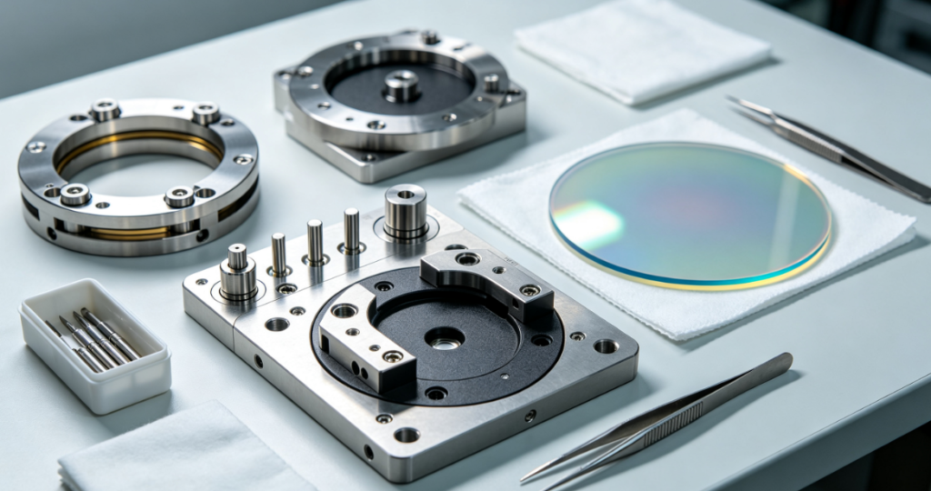
Wafer fixtures (also called wafer chucks, carrier plates, vacuum stages, wafer holders) are custom precision substrates that secure 100mm, 200mm, or 300mm silicon wafers through every fabrication step.
Critical functions that demand micro accuracy:
- Precision vacuum slot arrays to hold thin wafers without warping
- Ultra-flat reference surfaces for optical probing & metrology
- Micro alignment pin holes with near-zero positional deviation
- Recessed channels for cooling gas or fluid distribution
- Cleanroom-compatible smooth surfaces to avoid particle contamination
Tolerance benchmarks for industrial wafer fixtures:
- Flatness across full plate: ≤ 0.002 mm
- Position tolerance for alignment holes: ±0.001 mm
- Vacuum groove width consistency: ±0.0008 mm
- Surface roughness Ra ≤ 0.02 μm for contact surfaces
A regular CNC machine can’t reliably hit these specs. Its spindle runout, tool minimum size, and vibration levels create micro inconsistencies that damage delicate silicon wafers. Only dedicated micro CNC machining hardware and semiconductor-focused process controls lock in ultra-tight tolerances at scale.
Core Challenges Machining Wafer Fixtures
We’ve listed the biggest manufacturing hurdles semiconductor engineers face with wafer fixtures—and how micro CNC eliminates each issue:
- Micro feature geometry limitations Vacuum slots, micro fluid channels, and tiny alignment cutouts require micro end mills as small as 0.1mm. Standard CNC tools can’t reach narrow, shallow micro cavities without breaking cutters or leaving uneven wall surfaces.
- Thermal warpage risk Aluminum, titanium, and ceramic composite fixture stock expands with cutting heat. Micro CNC uses low-load trochoidal micro milling and constant temperature machine enclosures to stabilize material during cuts.
- Micro burr contamination hazard Even invisible micro metal slivers will contaminate cleanroom wafer batches. Conventional deburring scratches critical flat surfaces; micro CNC paired with precision ultrasonic deburring removes micro burrs without altering micron tolerances.
- Cross-axis positional drift Multi-axis standard machines have minor slide drift over long cutting cycles. Our micro 5-axis equipment features ultra-rigid granite bases to lock axis positioning for hours of continuous fixture production.
- Consistent ultra-smooth finish requirements Any uneven surface texture creates micro-scratches on wafer backings. Micro CNC fine passes cut surface roughness down to mirror levels before specialized semiconductor finishing.
Zorapid’s End-to-End Micro CNC Workflow for Wafer Fixtures
Our full micro CNC workflow is built specifically for semiconductor wafer fixture production, every stage optimized for micron-level accuracy. No outsourced secondary operations, zero tolerance drift between steps.
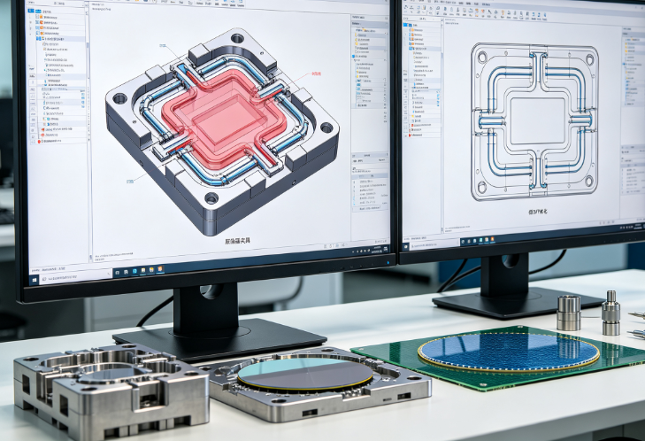
Micro DFM Analysis Tailored for Semiconductor Wafers
We kick off every project with a dedicated micro DFM review—free for all Zorapid clients. This step catches manufacturability risks before any material is cut, saving you rework and wafer yield loss later.
Our semiconductor DFM engineers deep-dive into:
- Micro slot & channel width vs available micro tool sizes
- Wall thickness around tiny vacuum grooves to prevent deflection
- Tolerance rationalization: flag over-specified non-critical features to cut machining time without sacrificing wafer contact precision
- Thermal expansion offsets calculated for aluminum, titanium, and ceramic fixture blanks
- Cleanroom finish compatibility pre-check (anodizing, passivation, electropolishing layer thickness adjustments)
- Deburring access planning for internal micro cavities
We send a full DFM report with annotated CAD revisions within 24 hours, including cost and lead time projections for prototype and production batches.
Ultra-Precision 5-Axis Micro CNC Machining
After DFM sign-off, we move to enclosed temperature-controlled micro CNC cells.
Key hardware specs for wafer fixture production:
- Granite machine base to eliminate vibration
- High-speed low-runout micro spindles (up to 80,000 RPM)
- Micro cutting tools ranging from 0.1mm to 2mm diameter
- Closed-loop linear scales with 0.0001mm positional feedback
- Constant 20°C internal machine temperature to block thermal expansion
We split machining into two controlled phases:
- Rough micro milling: Remove bulk material with light cutting loads to minimize stress-induced warpage
- Finish micro passes: Multiple shallow cutting layers to hit flatness, positional and dimensional ultra-tight tolerances
For complex 300mm wafer stages with multi-sided micro channel layouts, 5-axis micro CNC cuts all critical features in one single setup—eliminating re-fixturing alignment error that plagues 3-axis standard machining.
Burr-Free Micro Deburring & Critical Edge Control
Micro burrs are a cleanroom disaster for wafer processing. Our in-house micro deburring station uses ultrasonic media finishing and precision micro abrasive flow processing for internal vacuum grooves.
Process standards we follow:
- All micro channel edges radiused to 0.03mm minimum to prevent wafer edge chipping
- Zero raised burrs on vacuum slot walls and top contact surfaces
- No dimensional shift after deburring (we validate critical dimensions post-process)
- Full cleaning cycle to remove all micro abrasive particles before finishing
Semiconductor-Grade Surface Finishing
Wafer fixtures require specialized coatings that satisfy cleanroom, anti-corrosion, and low-particle requirements. All finishing runs in-house, calibrated to preserve micron tolerances:
- Hard coat anodizing (aluminum fixtures): Controlled thin oxide layer to avoid altering flatness specs
- Electropolishing: Mirror ultra-smooth Ra surfaces for direct wafer contact
- Stainless steel passivation: Anti-contamination treatment for probe station fixtures
- Non-conductive PTFE coating for electrostatic discharge sensitive wafer handling
We pre-compensate all micro CNC cuts to account for coating thickness, so finished fixtures still hit your original tolerance print exactly.
100% CMM Metrology Inspection for Micron Tolerances
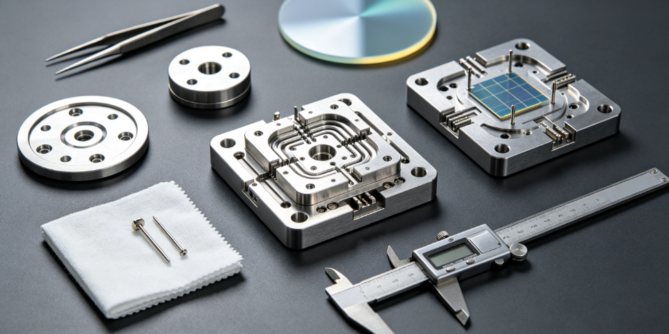
Every single wafer fixture undergoes full coordinate measuring machine (CMM) inspection before shipping—no batch sampling shortcuts for semiconductor hardware.
Our QA verification covers:
- Full surface flatness mapping across the entire fixture plate
- Positional tolerance check for all micro alignment holes
- Width & depth consistency of every vacuum micro channel
- Surface roughness testing on all wafer contact zones
- Coating thickness and adhesion validation
We deliver a full certified inspection report with CMM scan data, critical for fab quality compliance and audit records.
Top Materials Used for Micro CNC Wafer Fixtures
We machine wafer fixtures from cleanroom-grade stock, each material selected for specific semiconductor use cases:
- 6061 / 7075 Aluminum (Most Popular) Lightweight, high thermal conductivity, easy micro machining, hard anodizable. Ideal for vacuum chucks, transport wafer carriers, low-temperature processing stages.
- Titanium Alloy Low thermal expansion, corrosion-resistant, non-magnetic. Perfect for high-temperature deposition, plasma etching, and sensitive optical inspection fixtures.
- 316L Stainless Steel Ultra-clean, particle-free, chemical resistant. Used for wet processing wafer fixtures and lab test probe holders.
- PEEK / ULTEM Engineering Plastics Non-conductive, low friction, anti-static options for ESD-sensitive thin wafer handling fixtures. Limited to lower-temperature processes.
Real Client Case: 200mm Wafer Vacuum Chuck Fixture Production
A semiconductor equipment OEM reached out to Zorapid needing prototype and small-batch 200mm aluminum vacuum chucks for their new wafer probing station.
Client Pain Points
- Previous supplier used standard CNC, failed flatness tolerance of ≤0.002mm across the 200mm plate
- Visible micro burrs in vacuum slots caused repeated silicon wafer scratching during testing
- Outsourced finishing created inconsistent anodizing thickness, throwing off critical dimensions
Zorapid Micro CNC Solution
- Micro DFM analysis adjusted vacuum slot radii and optimized material stock thickness to reduce warpage
- Temperature-controlled 5-axis micro CNC machining with multi-stage fine finishing passes
- Ultrasonic micro deburring removed all micro slivers without altering channel geometry
- Calibrated thin hard coat anodizing with pre-cut dimensional compensation
- 100% full-plate CMM flatness mapping for every chuck
Final Result
All prototype fixtures hit every micron tolerance spec on the first run. Wafer scratch incidents dropped to zero during client lab testing, and total project lead time cut by 35% compared to their fragmented multi-vendor workflow. The OEM now orders monthly production batches through our micro CNC line.
Micro CNC vs Regular CNC: Side-by-Side Comparison
| Parameter | Micro CNC Machining (Wafer Fixture Grade) | Standard Conventional CNC |
|---|---|---|
| Minimum Tool Diameter | 0.1 mm micro end mills | ≥1.0 mm standard cutters |
| Standard Tolerance Range | ±0.0005 ~ ±0.002 mm | ±0.01 ~ ±0.05 mm |
| Machine Base | Vibration-dampened granite | Cast metal base (minor vibration) |
| Spindle Speed | Up to 80,000 RPM low-runout | Max 12,000–24,000 RPM |
| Thermal Control | Full enclosed temperature stabilization | No controlled machine environment |
| Suitable Parts | Wafer chucks, micro fluid channels, probe fixtures, ultra-precision semiconductor hardware | Generic brackets, structural frames, low-tolerance mechanical parts |
| Surface Roughness Baseline | Ra ≤ 0.02 μm post-finish | Ra 1.6–6.3 μm as-machined |
| Risk of Micro Burrs | Minimal with dedicated micro deburring | High risk of invisible micro slivers |
FAQ
What wafer sizes can Zorapid’s micro CNC produce fixtures for?
We support 100mm, 200mm, and 300mm standard silicon wafer fixtures, plus custom small-format lab wafer carriers for R&D prototype testing.
Can micro CNC handle ceramic or composite wafer fixture blanks?
Yes. Our micro CNC cell has specialized low-pressure cutting parameters for ceramic and metal matrix composite stock for high-temperature wafer processing equipment.
Is micro CNC only for prototype batches, or can you run production volumes?
Our micro CNC lines support 1-off R&D prototypes all the way through medium-volume production runs for OEM equipment manufacturing. The same micron tolerance standards apply regardless of order size.
How long does micro CNC production for a wafer chuck fixture take?
Standard prototype turnaround: 5–8 business days including DFM, micro machining, finishing and full CMM inspection. Larger batch production lead times are quoted based on quantity and fixture complexity.
Can you design custom micro vacuum slot patterns for specialized wafer processes?
Our in-house semiconductor design team can collaborate with your process engineers to optimize micro vacuum channel layouts, pressure distribution, and edge holding geometry fully compatible with your etching, probing or deposition tools.
Wrap-Up
Wafer processing yield hinges entirely on the micron-level precision of your holding fixtures. Standard machining shops can’t deliver the stability, micro feature control, and cleanroom-grade finishing semiconductor manufacturing demands.
Zorapid’s dedicated micro CNC machining service was built from the ground up for ultra-tight tolerance wafer fixtures. From free micro DFM design optimization to vibration-controlled micro cutting, burr-free finishing and full CMM certification, we own every stage of production to eliminate tolerance drift, particle contamination, and costly wafer damage.
Whether you’re developing a new lab prototype chuck or scaling medium-volume wafer carrier production for fab equipment, our semiconductor-focused engineering team will deliver consistent, print-perfect micro CNC parts on schedule.
Request Your Free Micro DFM & Multi-Part Quote Today
Send your fixture CAD files, tolerance prints, and wafer process requirements to our precision manufacturing team. We’ll complete a full micro manufacturability review, outline material recommendations, and share a transparent all-in quote covering micro CNC machining, finishing and full metrology inspection.