Published:Zorapid.Ltd
Let’s talk about the unsung heroes of the semiconductor world.
You’ve got your wafers, your chips, your fancy cleanrooms. But none of it works without the tiny, precision-machined pins and terminals that carry the signals. Those little copper and brass parts? They make or break the whole system.
Get them wrong, and you’re looking at signal loss, overheating, or total test failure. Get them right? Everything just works.
If you’re sourcing conductive terminals for semiconductor equipment, this is your complete guide. We’re breaking down everything from material selection to tolerances to why CNC turning beats every other method for these critical parts.
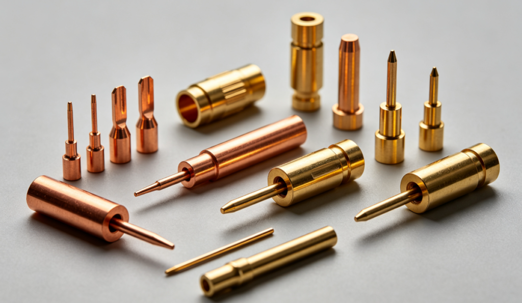
Why Copper and Brass? The Science Behind the Pins
Let’s start with the basics. Why do we use copper and brass for semiconductor terminals instead of, say, steel or aluminum?
It all comes down to three things: conductivity, machinability, and durability.
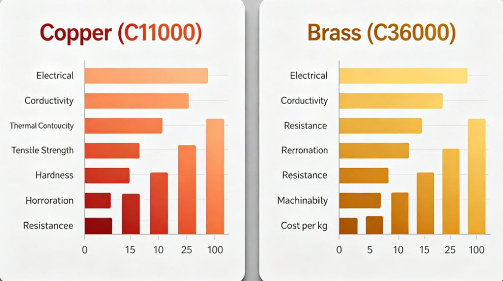
Copper (C11000) — The Conductivity King
Pure copper is basically electricity’s best friend. Here’s what makes it special:
- 58 MS/m electrical conductivity — that’s 97% IACS, second only to silver
- 401 W/m·K thermal conductivity — heat dissipates fast, no hot spots
- Excellent formability — you can bend it, crimp it, shape it without cracking
- Natural corrosion resistance — forms a protective oxide layer
The catch? Pure copper is soft. Really soft. For high-cycle applications like test sockets, it can wear out faster. That’s where brass steps in.
Brass (C36000) — The Machining Marvel
Is copper + zinc, and it’s basically made for CNC turning.
- Free-machining properties — chips break cleanly, no stringy mess
- Higher hardness than pure copper — stands up to more mating cycles
- Good conductivity — not as good as pure copper, but still way better than steel
- Lower cost — saves you money without sacrificing too much performance
Brass is the workhorse of the terminal world. If you need millions of parts fast and consistent, brass is usually your answer.
Why CNC Turning Is the Only Way to Go for Semiconductor Terminals
You could stamp these parts. You could cast them. But for semiconductor-grade quality? CNC turning is non-negotiable.
Here’s why:
1. Tighter Tolerances Than Your Tightest Deadline
Semiconductor terminals aren’t close enough parts. We’re talking:
- Diameter tolerances down to ±0.005mm — that’s 5 microns, thinner than a human hair
- Concentricity within 0.003mm — the pin has to be perfectly centered
- Surface finish Ra < 0.4μm — smooth enough that contact resistance stays consistent
- Length tolerances of ±0.01mm — every pin has to seat exactly right
Stamping can’t hit those numbers. Casting? Forget about it. Only CNC turning delivers this level of precision, part after part, million after million.
2. Consistency That Doesn’t Quit
In semiconductor manufacturing, one bad terminal can take down an entire test run. That’s why consistency isn’t a nice-to-have — it’s everything.
CNC turning delivers:
- Identical parts every single time — the first part matches the 100,000th
- No tooling wear surprises — we monitor tool life and replace before drift happens
- Statistical process control — Cpk > 1.33 on all critical dimensions
- Full traceability — every batch comes with material certs and inspection data
3. Design Freedom That Lets You Innovate
Got a weird terminal shape? A custom flange? A unique groove pattern? CNC turning laughs at complexity.
Unlike stamping, which needs expensive custom dies, CNC turning just needs a program change. Want to iterate on a design? Send us the new CAD file, and we’re making parts the same day.
That speed to iterate? It’s how semiconductor companies stay ahead.
Copper vs. Brass: How to Pick the Right One
This is the question we get every day. Should I use copper or brass for my terminals?
The answer depends on what matters most for your application.
Choose Copper If:
- Maximum conductivity is critical — high-frequency signals, high-current applications
- Thermal management is a concern — parts that run hot need to dissipate heat fast
- Corrosion resistance matters most — harsher environments, longer service life
- You’re plating with gold or silver — copper takes plating beautifully
Choose Brass If:
- Machining speed and cost matter — brass machines 30% faster than copper
- Higher wear resistance is needed — test sockets with high mating cycles
- You need strength with conductivity — structural + electrical in one part
- Volume is high — millions of parts where every cent counts
Pro Tip: You Don’t Always Have to Choose
Many semiconductor designs use both. Brass for the structural body, copper for the contact tip, or vice versa. The best solution depends on your exact requirements.
Not sure which is right for your project? Send us your specs, and we’ll tell you straight — no sales pitch, just engineering advice.
The Real Challenges in Semiconductor Terminal Manufacturing
Anyone can turn a brass pin. But semiconductor-grade terminals? That’s a different game.
Here are the real challenges, and how we tackle them:
1: Surface Finish That Actually Matters
A rough surface doesn’t just look bad — it increases contact resistance, causes signal loss, and accelerates wear.
Our solution:
- Diamond-tipped tooling for mirror finishes on contact surfaces
- Ra < 0.4μm standard, Ra < 0.2μm available for high-frequency apps
- Post-machining vibratory finishing for burr-free edges
- 100% visual inspection under magnification
2: Cleanliness Is Next to Godliness
In semiconductor, even tiny particles can cause failures. A single chip of brass stuck in a test socket? That’s a scrapped wafer.
Our solution:
- Ultrasonic cleaning in multiple stages
- Class 100 cleanroom packaging
- Vacuum-sealed ESD-safe bags
- Particle count verification per batch
3: Plating Adhesion That Doesn’t Flake
Most terminals get plated — gold, silver, tin, nickel. But if the base surface isn’t perfect, the plating flaks off, and you’ve got a problem.
Our solution:
- Controlled surface roughness for plating adhesion (Ra 0.2-0.4μm sweet spot)
- Pre-plating activation treatment
- Plating thickness verification via XRF
- Adhesion testing per ASTM B571
4: Keeping Up with Wafer Probe Demand
Semiconductor test sockets need hundreds — sometimes thousands — of pins, all identical, all perfect. And they need them fast.
Our solution:
- Swiss-type CNC lathes with bar feeders for lights-out production
- 12,000+ RPM spindles for fast, clean cuts
- In-process gauging that checks every part
- Capacity to scale from prototypes to 100k+ parts per month
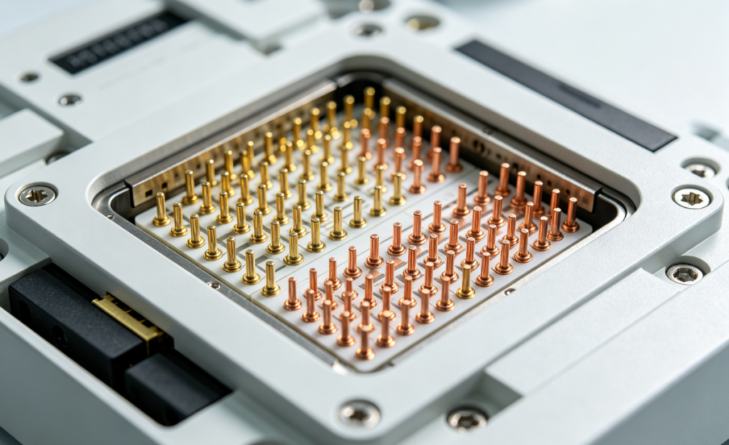
Real-World Example: 50,000 Test Socket Pins in 10 Days
A semiconductor test equipment company came to us with a problem. Their current supplier was 4 weeks late on a batch of brass test pins. Their customer was breathing down their neck.
The specs:
- Material: C36000 free-machining brass
- 0.8mm diameter pin with 0.02mm tolerance
- 3mm length with ±0.01mm accuracy
- Gold plating 0.5μm over nickel underplate
- Quantity: 50,000 pieces
Here’s how we delivered:
- Day 1: DFM review — found one edge that could cause plating issues, suggested a 0.05mm radius
- Day 2: Approved the optimized design, ordered material
- Days 3-5: First article inspection + approval + full production setup
- Days 6-8: Full production run on 4 Swiss-type lathes
- Day 9: Gold plating + ultrasonic cleaning + inspection
- Day 10: Packed in cleanroom, shipped via air freight
Total time: 10 days from PO to delivery. Their test equipment build stayed on schedule. Their customer never knew there was a problem.
And the quality? Cpk of 1.67 on the critical diameter. Zero rejects in incoming inspection.
The Zorapid Advantage
You might be thinking, “Lots of shops do CNC turning.” Fair. But here’s what makes us different for semiconductor work.
Speak Semiconductor
We don’t just machine parts — we understand what they’re for. Know why contact resistance matters. We know what Class 100 means. We know the difference between a probe pin and a terminal pin.
You won’t have to explain basic semiconductor concepts to us.
Have the Right Equipment
- Swiss-type CNC lathes with sub-spindles for complete parts in one operation
- High-precision tooling with runout < 0.001mm
- In-process measurement systems
- Cleanroom packaging facility
Control the Whole Process
From raw material certs to final packaging, everything happens in our facility. No outsourcing, no handoffs, no surprises.
We’re Certified for This
- ISO 9001:2015
- IATF 16949 (automotive grade, which is overkill for most semi apps)
- RoHS and REACH compliant materials
- Full material traceability
FAQ
What’s the typical lead time for copper and brass terminals?
For standard parts, 7-10 days. For prototypes, we can often turn samples in 3-5 days. High-volume runs (100k+) usually take 2-3 weeks. We’ll give you an exact date with your quote — no vague “2-4 weeks” nonsense.
What tolerances can you hold?
For diameters, we regularly hold ±0.005mm (5 microns) on production parts. For prototypes, we can go tighter if needed. Length tolerances are typically ±0.01mm. Concentricity within 0.003mm. Surface finish Ra < 0.4μm standard, Ra < 0.2μm available.
Do you offer plating services?
Yes. We work with certified plating partners and manage the whole process. Common options: gold (0.1-2μm), silver, tin, nickel, electroless nickel. We can do selective plating too — only on the contact areas — to save you money.
What’s the minimum order quantity?
One. Seriously. We do everything from single prototype pins to 100,000+ piece production runs. No order is too small. Pricing gets better at volume, but we’re happy to quote 5 pieces if that’s what you need.
Can you work from my CAD files?
Absolutely. We accept STEP, IGES, SolidWorks, and just about any other CAD format. If you only have a 2D drawing, that works too. We’ll review it and come back with any DFM suggestions before we quote.
How do you ensure consistency across large batches?
Three ways. First, we use Swiss-type lathes with bar feeders — the same tooling, same program, every part. Second, we do in-process sampling every 30 minutes with SPC charting. Third, we do 100% inspection on critical dimensions for semiconductor-grade parts. Cpk > 1.33 is our standard.
Do you provide material certifications?
Yes, every batch comes with full material certs (mill test reports) showing chemical composition and mechanical properties. We can also provide inspection reports, plating thickness data, and whatever documentation your quality team needs.
What copper and brass alloys do you work with?
Most common: C11000 (pure copper), C10100 (oxygen-free copper), C36000 (free-machining brass), C3604, C26000 (cartridge brass). We also work with beryllium copper (C17200) for high-strength, high-conductivity apps. Need a specific alloy? Just ask.
Can you make custom terminal designs?
That’s basically all we do. Every customer has unique requirements. Custom lengths, custom diameters, special grooves, flanges, steps, undercuts — if you can draw it, we can probably turn it. And if you can’t draw it? Send us a sketch or a sample, and we’ll figure it out.
How do you handle packaging for semiconductor use?
All semiconductor-grade parts get ultrasonic cleaning, then packaged in our Class 100 cleanroom. We use ESD-safe trays or vacuum-sealed bags, depending on the part. Particle counts are verified before shipment. If you have specific packaging requirements, we can accommodate them.
What industries do you serve besides semiconductor?
Semiconductor is a big one, but we also do a lot of medical devices, aerospace, automotive electronics, and telecom. The precision requirements are similar across all of them — tight tolerances, consistent quality, full traceability.
How do I get a quote?
Send us your drawing or CAD file, tell us the quantity and any special requirements (plating, packaging, etc.). We’ll get back to you with a detailed quote and lead time within 24 hours. No obligation, no sales call unless you want one.
Ready to Get Better Terminals?
If you’re tired of:
- Suppliers who miss deadlines
- Parts that don’t meet spec
- Incoming inspection rejects
- Having to explain basic semiconductor requirements over and over
Then let’s talk.
Send us your drawings today. We’ll review them, suggest any DFM improvements that will save you time and money, and send you a real quote with a real delivery date.
No fluff. No excuses. Just precision copper and brass terminals, delivered on time, every time.
Zorapid — Precision CNC Turning for Semiconductor Excellence
ISO 9001:2015 Certified | RoHS & REACH Compliant | Full Material Traceability
3000㎡ Smart Manufacturing Center | Zhongshan, Guangdong