Published by Zorapid
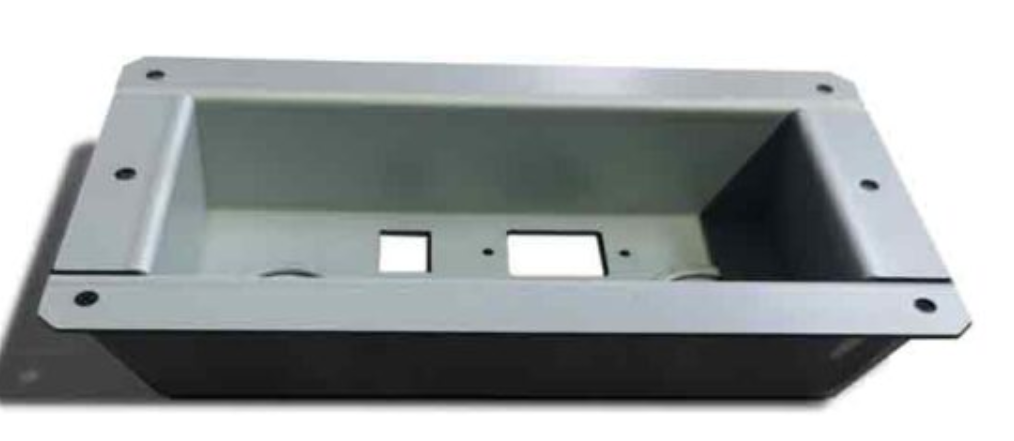
Electronic and semiconductor enclosures aren’t just metal boxes—they need precise EMI shielding, controlled thermal dissipation, cleanroom compatibility, tight PCB fit tolerances, corrosion resistance, and stable grounding paths all at once. Many hardware designers draft CAD without sheet metal manufacturing constraints, leading to bent distortion, poor shielding gaps, assembly misalignment, scrap, and delayed product launches.
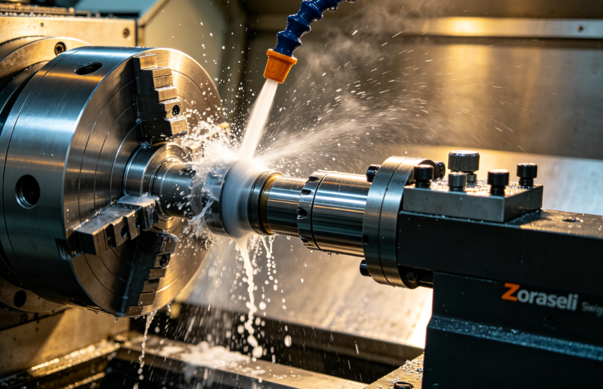
Most sheet metal fabricators only follow generic bend rules; they lack deep experience with semiconductor cleanroom specs, EMI gasket mating, precision PCB standoff alignment, and low-particulate finishing. At Zorapid, our integrated laser cut, CNC bend, robotic rivet, in-house anodize/powder coat production line is built exclusively for high-spec electronics & semiconductor housings, with a fully validated library of design rules tuned for shielding, thermal transfer, and cleanroom compliance. Today we break down critical design standards, competitor limitations, material performance, real semiconductor customer cases, lead time benchmarks, and 2026 industry manufacturing trends.
In-Depth Professional Process Technical Analysis + Competitor Benchmark
Non-Negotiable Core Design Rules for Electronics/Semiconductor Sheet Metal Enclosures
Rule 1: Bend Radius & Minimum Flange Height (Eliminate Cracked, Distorted Edges)
- Standard 5052/6061 Aluminum: Min inside bend radius = 1× sheet thickness (t); semiconductor thin gauge 0.8–1.2mm strictly 1t minimum
- 304 Stainless Cleanroom Grade: Min radius = 1.2t (stainless higher tensile strength cracks easily on tight bends)
- Minimum usable flange length: ≥3t; shorter flanges cannot be clamped by press brake dies, resulting in tilted, uneven bent walls Common competitor mistake: Designers specify 0.5t sharp radii for compact sizing; fabricators force bend and create micro-cracks that break shielding continuity and release metal particulates dangerous for semiconductor wafers.
Rule 2: EMI Shielding Gap Control (Max 0.2mm Continuous Contact Gap)
Electromagnetic interference leaks through parting line gaps; semiconductor test gear requires Class A shielding performance:
- All mating seams, lid frames, flange overlaps must hold gap ≤0.2mm across full length
- Gasket mounting ledges need flatness ±0.05mm per 300mm to compress conductive foam/gaskets evenly
- Rivet spacing max 25mm along shielding flanges to prevent panel bowing and gap opening under thermal cycling Budget shops ignore flatness control; uneven panels create 0.5–1mm gaps that destroy shielding effectiveness.
Rule 3: PCB Standoff & Threaded Insert Precision Alignment
Semiconductor control boards, sensor PCBs demand positional tolerance ±0.08mm for standoffs/self-clinching hardware:
- Standoff hole location locked via unified laser-cut datum—no post-bend re-drilling (drilling after bending shifts positions)
- Blind tapped holes minimum depth = 1.5× thread diameter for stable grounding
- Robotic clinch insertion with calibrated compression force to avoid sheet bulging (bulges lift PCBs and break ground contact)
Rule 4: Thermal Dissipation Geometry Rules
High-power RF, power supply, semiconductor driver enclosures rely on aluminum heat transfer:
- Extended bent heat sink fins minimum thickness 1.0mm, fin gap ≥2t to prevent bend deformation
- Internal mounting bosses for thermal interface material (TIM) must be coplanar ±0.04mm to ensure full TIM contact
- Avoid isolated thick solid blocks—uniform sheet thickness enables even heat spread across chassis
Rule 5: Cleanroom Low-Particulate Design Standards (Semiconductor Fab Critical)
- All edges fully automated deburr; no sharp micro-slivers that shed particles onto wafers
- Weld joints ground smooth, no porous rough weld crevices that trap dust/chemical residue
- Anodize seal must be pore-sealed completely; un-sealed porous oxide traps cleanroom contaminants
- External fastener recesses designed for easy IPA wipe-down, no deep hidden pockets
Rule 6: Tolerance Stack-Up for Multi-Panel Riveted Assemblies
Full enclosure assemblies (base + lid + internal support frames) use one single CAD datum origin for all laser cut blanks:
- Linear dimensional tolerance ±0.1mm standard; semiconductor test gear tightened to ±0.06mm
- Angular bend tolerance ±0.1° to keep lid/flange mating faces perfectly parallel
Zorapid Full Electronics Enclosure Integrated Workflow
- Pre-production DFM design rule audit: We flag bend radius, flange, gap, standoff, cleanroom violations with annotated CAD revisions within 24hrs
- AI nesting laser cutting with automated brush deburr (100% edge sliver elimination)
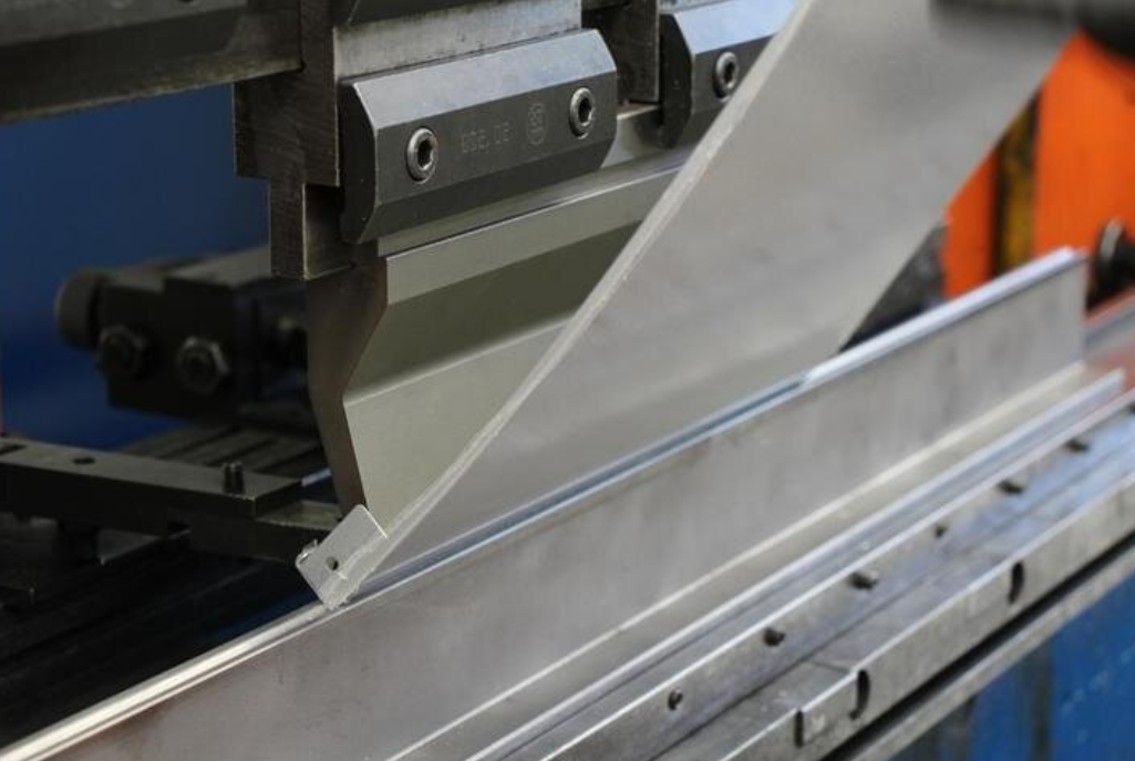
- 8-axis CNC bending with material-specific springback compensation calibrated for Al/stainless electronics grades
- Vision-guided robotic clinch/rivet assembly with force monitoring for standoffs/shield flanges
- Climate-controlled in-house finishing: Type II hard-seal anodize, low-particulate powder coat, passivation for stainless
- Full CMM flatness/gap/positional inspection + EMI shielding validation sampling for critical semiconductor batches
Competitor Fabrication Performance Benchmark Table
| Supplier Tier | Enclosure Flatness Tolerance | Average Shielding Gap Max | Cleanroom Particulate Pass Rate | Assembly Defect Rate |
|---|---|---|---|---|
| Budget General Sheet Metal Shop | ±0.18mm /300mm | 0.5–0.9mm | 62% (high micro-sliver risk) | 5.3%–8.1% |
| Mid-Tier Standard Electronics Fabricator | ±0.10mm /300mm | 0.25–0.4mm | 84% | 2.2%–3.8% |
| Zorapid Semiconductor/Electronics Precision Line | ±0.04–0.06mm /300mm | ≤0.2mm certified full seam | 99.2% zero sliver pass | 0.32%–0.68% |
Unsolvable Enclosure Challenges Competitors Cannot Resolve — Zorapid Custom Solutions
Challenge 1: Small Semiconductor Wafer Test Chamber Enclosure (0.8mm 5052 Al, Class 100 Cleanroom, 60dB EMI Shielding)
Competitor Failure: Generic bending created micro-edge slivers failing cleanroom particulate testing; uneven lid gaps dropped shielding to only 38dB; rework grinding added more contaminants. Third-party anodize had incomplete pore sealing.
Zorapid Solution:
- DFM adjusted all internal bend radii to strict 1t minimum, eliminated ultra-short flanges
- Dual-stage automated laser edge deburr + ultrasonic pre-finish wash
- Synchronized robotic rivet spacing 20mm max along shielding flanges to hold gap ≤0.18mm
- Climate-controlled Type II nickel acetate sealed anodize (zero open pores for cleanroom washdown) Result: 62dB shielding performance, Class 100 cleanroom particulate certification, 0.41% batch defect rate.
Challenge 2: Multi-Panel Stacked RF Telecom Enclosure (Mixed 5052 Al frame + 304 stainless cleanroom inner shield inserts)
Competitor Failure: Different springback values for aluminum and stainless created mismatched mating flanges, 0.4–0.7mm gaps breaking RF performance; separate vendor finishing caused color mismatch on assembled units.
Zorapid Fix:
- Separate MES springback offset profiles loaded for Al and stainless blanks in one project file
- Unified datum origin for all mixed-material panels to lock flange positional alignment
- Matched passivation/anodize finishing cycles scheduled sequentially in-house for uniform cosmetic & shielding properties
- CMM paired gap inspection across full assembly stack before packaging
Challenge 3: High-Power EV Semiconductor Inverter Enclosure (Thermal TIM base plane, 1.5mm 6061-T6 aluminum)
Competitor Failure: Bent base plate bowed ±0.15mm; TIM could not make full contact, thermal runaway risk for power semis; standoffs bulged from uncalibrated clinch force, PCB misalignment.
Zorapid Fix:
- Pre-stress relief leveling of 6061 blanks before bending to eliminate plate bow
- CNC secondary fly-cut finish on TIM mounting plane to lock coplanarity ±0.03mm
- Servo-controlled robotic clinch pressure matched to 1.5mm gauge to prevent sheet deformation around standoffs
Challenge 4: Ultra-Thin 0.6mm Stainless Mini Semiconductor Sensor Housings (Tiny 2mm short flanges for compact footprint)
Competitor Failure: Standard press brake cannot safely bend 2mm flanges on 0.6mm stainless; parts crack or tilt at bend lines, scrap rate >12%.
Zorapid Fix: Custom segmented micro bend dies engineered for ultra-short thin-gauge flanges; slow low-pressure bend cycles with real-time angle feedback to eliminate cracking and tilt.
Challenge 5: Hermetic-Sealed Semiconductor Test Box Requiring Vacuum Leak-Tight Rivet Joints
Competitor Failure: Hand riveting creates inconsistent clamp load; helium leak test fails at 1×10⁻⁶ mbar·L/s threshold.
Zorapid Fix: Closed-loop force-displacement robotic riveting with programmed compression curves; 100% helium leak sampling per batch, archive force curve QA logs for semiconductor audit compliance.
Applicable Materials & Electronics/Semiconductor Enclosure Performance Comparison
| Material Grade | Standard Gauge Range | EMI Shielding Efficiency (1–10GHz) | Cleanroom Compatibility | Thermal Conductivity W/mK | Zorapid Average Defect Rate | Primary Best Fit Application |
|---|---|---|---|---|---|---|
| 5052-H32 Aluminum | 0.8–3.0mm | Excellent 55–65dB | Very Good (sealed anodize) | 138 | 0.32% | Standard test equipment, telecom, low-medium power semis |
| 6061-T6 Aluminum | 1.2–4.0mm | Excellent 58–68dB | Very Good | 167 | 0.38% | High-power inverter, thermal heat spread chassis, heavy structural frames |
| 304 Stainless Steel | 0.6–2.5mm | Good 45–55dB | Elite (passivated zero contamination) | 16 | 0.62% | Wafer fab cleanroom inner shields, corrosive chemical process enclosures |
| 316L Stainless Steel | 1.0–2.0mm | Good 42–52dB | Premium chemical resistance | 13 | 0.70% | Wet etch semiconductor process equipment, offshore sensor housings |
| Galvanized GI Steel | 1.0–3.0mm | Fair 35–45dB | Poor (zinc flaking particulates) | 60 | 0.35% | Non-cleanroom low-budget industrial control boxes only |
Key Material Design Rules for Semiconductor/Electronics:
- Aluminum is #1 for balanced shielding + thermal transfer; 6061-T6 selected when high heat dissipation is priority
- 304/316 stainless mandatory for Class 100/1000 cleanroom wet process zones—anodized aluminum cannot withstand aggressive semiconductor cleaning chemistries long-term
- Galvanized steel banned entirely for wafer/fab environments due to zinc particulate shedding risk
- Thin 0.6–0.8mm gauges restricted to low-power mini sensor housings; power chassis minimum 1.2mm aluminum for rigidity under thermal cycling
Real Customer Case Study
Case 1: US Semiconductor OEM Class 100 Wafer Test Chamber Assembly
Project Scope: 12,000 unit batch, 0.8mm 5052 aluminum multi-part enclosure, 60dB EMI requirement, Class 100 cleanroom particulate spec, ±0.08mm PCB standoff tolerance
Previous Multi-Vendor Pain Points: Laser/bend shop outsourced anodizing; unregulated deburr left micro slivers (failed cleanroom test), average lid shielding gap 0.52mm (only 39dB shielding), total assembly scrap 6.7%, 13-day delivery delay across three suppliers, fragmented QA documentation for semiconductor audit.
Zorapid One-Stop DFM & Manufacturing Execution
- Free pre-production DFM design rule overhaul, adjusted bend radii/flange lengths to eliminate high-risk geometry
- AI nested laser cutting + two-stage automated brush deburr for full edge particulate elimination
- 8-axis CNC bending with 5052 calibrated springback profiles, ±0.1° angular tolerance
- Vision robotic rivet/standoff insertion with force monitoring to prevent sheet bulging
- In-house climate-controlled fully sealed Type II anodize, ultrasonic cleanroom wash cycle post-finish
- Full batch gap flatness CMM scanning, EMI shielding sample testing, independent particulate lab certification
Measurable Production Outcomes
- Final assembly reject rate dropped to 0.41%
- Max shielding gap locked ≤0.18mm, certified 62dB shielding across full frequency band
- Passed Class 100 cleanroom airborne particle count on first submission
- Total lead time cut from 38 days (3 vendors) down to 15 days
- Consolidated semiconductor audit package: mill certs, CMM logs, shielding/particulate test reports
- Case 2: EU Power Semiconductor Inverter Chassis (6061-T6 Thermal Base Plate)
Your Production Pain Points → Zorapid Tailored Enclosure Design & Fabrication Solutions
Pain 1: CAD designs fail manufacturing due to too-tight bend radii, tiny flanges, unoptimized shielding geometry
Solution: Free pre-order DFM design rule audit; annotated CAD revision pack fixing bend, flange, gap, standoff, cleanroom risks within 24 business hours
Pain 2: Multi-supplier split fabrication creates misaligned panels, uneven shielding gaps, poor cleanroom finish
Solution: Single-source laser → bend → rivet → anodize/passivate full workflow, one unified CAD datum for all assembly panels
Pain 3: Thermal base plates bow, TIM cannot make full contact risking semiconductor overheating
Solution: Pre-blank stress relief leveling, secondary CNC fly-cut finishing to lock coplanarity to ±0.03mm
Pain 4: Thin stainless mini housings crack during bending from generic die tooling
Solution: Custom micro segmented bend dies, low-pressure slow bend cycles tuned for 0.6–1.0mm stainless thin gauge
Pain 5: Vacuum/helium leak test failures on sealed semiconductor test boxes from inconsistent rivet clamp load
Solution: Closed-loop force-monitored robotic riveting, 100% batch helium leak sampling with archived force curve QA logs
Pain 6: No compliant audit documentation stack for semiconductor fab, ISO 9001 / SEMI S2 cleanroom requirements
Solution: 10+ year encrypted storage of mill test certs, CMM flatness/gap data, shielding/particulate/leak test reports fully exportable for regulatory audits
2026 Global Industry Data & Future Trend Analysis
Enclosure Fabrication Quality & Cost Market Benchmark Table
| Production Supply Model | 2026 Average Assembly Defect % | Average Full Workflow Lead Time | Total Project TCO vs Baseline | 2026 Market Share |
|---|---|---|---|---|
| Fully split multi-vendor fabrication + external coating | 5.9% | 31–47 business days | 100% baseline cost | 38% low-end consumer electronics |
| Mid-tier partial in-house sheet + outsourced finishing | 2.8% | 21–31 business days | 92% relative spend | 40% standard industrial electronics |
| Zorapid integrated DFM-sheet-finish semiconductor-grade line | 0.50% average | 12–20 business days | 83–88% lower TCO (less scrap/rework/admin) | 22% fast-growing semiconductor, power semi, high-end RF test gear segment |
Key 2026–2030 Industry Trends Shaping Enclosure Design & Manufacturing
- SEMI Cleanroom Design Rules Become Standard for All Fab Hardware: By 2028, 64% of global semiconductor fabs will mandate pre-production DFM particulate risk audits; generic sheet shops without cleanroom finishing capacity lose fab hardware bids.
- Higher Frequency RF (10GHz+) Tightens EMI Gap Tolerance: Older 0.4mm acceptable gaps will drop to ≤0.2mm minimum for next-gen 5G/radar/semiconductor test gear, requiring precision flatness control only integrated lines can deliver.
- 6061-T6 Thermal Aluminum Enclosure Demand Surges: Power semiconductor and EV inverter growth pushes demand for high-thermal-conductivity precision base plates with coplanarity ±0.03mm specs.
- Single-Source Vertical Integration Preferred by Semiconductor OEMs: Supply chain risk reduction post-shortage drives buyers away from fragmented 3+ vendor chains to one-stop precision fabricators like Zorapid.
- Total Cost of Ownership Replaces Per-Pound Sheet Pricing: Procurement now calculates scrap rework, fab downtime from bad enclosures, and audit admin labor; low-defect integrated manufacturers deliver clear long-term cost advantages.
Core Zorapid Application Scenarios for Electronics & Semiconductor Custom Enclosures
Aluminum 5052 / 6061 Enclosure Lines
- Semiconductor wafer test chambers, probe station control housings (Class 100/1000 cleanroom)
- RF telecom base station shielding cabinets, 5G signal filter chassis
- Automotive power semiconductor inverter, onboard charger thermal frames
- Medical diagnostic electronics control boxes, laboratory test instrument housings
304 / 316L Stainless Cleanroom Enclosures
- Wet etch, deposition, plasma process inner shield housings for semiconductor fabs
- Corrosion-resistant chemical delivery equipment frames
- Ultra-pure DI water distribution control boxes, sterile lab instrument trays
Mixed-Material Hybrid Assemblies
Aluminum outer structural chassis + stainless internal cleanroom shielding inserts, pre-assembled and shipped ready for PCB integration
Delivery Speed Benchmarks & Full Enclosure Production Timeline
12,000pc Semiconductor 5052 Test Chamber Batch Lead Time Comparison
| Supplier Structure | Full Laser/Bend/Rivet/Anodize Lead Time | Rework Scrap Delay Risk | Consolidated Audit Documentation |
|---|---|---|---|
| Three split standalone vendors | 36–44 days | 10–17 day particulate/shielding rework hold | Three separate report bundles |
| Mid-tier two-process shop (finish outsourced) | 23–31 days | 4–8 day minor fit touch-up lag | Two document sets |
| Zorapid fully integrated one-stop line | 13–19 days | <1 day minor polish/QA adjustment risk | Single full SEMI/ISO audit package |
Standard Zorapid Step-by-Step Production Timeline
- DFM semiconductor design rule review & CAD optimization sign-off: 1 business day
- AI nested fiber laser cutting + automated full edge deburr: 2–4 days
- CNC precision bending with alloy springback calibration: 2–3 days
- Vision robotic rivet/clinch standoff assembly + leak test sampling (sealed units): 2–3 days
- Climate-controlled anodize/passivation + cleanroom ultrasonic wash: 2–3 days
- CMM gap/flatness inspection, shielding/particulate lab testing, certification packaging: 1 day
Expedited 8–10 day fast-track rush service available for critical semiconductor fab launch timelines; DFM deburr and sealing steps are never shortened to cut particulate or shielding performance.
Key Benefits of Partnering With Zorapid for Semiconductor & Electronics Enclosures
- Single Source Full Accountability: No finger-pointing between laser, bend, coating subcontractors; Zorapid absorbs all rework cost for shielding, particulate, fit defects
- Semiconductor-Tuned DFM Engineering Library: Pre-validated bend, flange, EMI gap, cleanroom design rules built from thousands of fab enclosure projects
- In-House Climate-Controlled Finishing Line: Sealed low-particulate anodize and stainless passivation, no third-party coating contamination risks
- Full Global Compliance Stack: ISO9001, IATF16949 power semi, SEMI S2 cleanroom compatible; full mill, CMM, shielding, particulate, leak test records archived long-term
- Closed-Loop Robotic Assembly: Force-monitored rivet/clinch insertion eliminates sheet bulging, standoff misalignment, inconsistent vacuum seal clamp load
- Mixed Aluminum/Stainless Expertise: Separate calibrated springback and finishing profiles for hybrid assembly chassis/shield sets
- Fluent English Electronics/Semi Application Engineers: Free pre-project CAD DFM risk assessment before any metal cutting begins
- Global Door-to-Door Shipment Support: Complete customs compliance paperwork, air freight coordination direct to US/EU semiconductor fabs and electronics OEM facilities
Summary
Many electronic and semiconductor enclosure failures trace back to unoptimized sheet metal CAD designs built without manufacturing, EMI, thermal, and cleanroom constraints. Generic fabricators apply one-size-fits-all bend and finishing processes, leading to cracked panels, large shielding gaps, dangerous metal particulates for wafer processing, misaligned PCB mounting, and costly scrap/rework across multi-vendor supply chains.
Zorapid’s fully integrated DFM → laser cut → CNC bend → robotic assembly → controlled finishing workflow uses semiconductor-grade validated design rules, alloy-specific machining calibrations, and in-house performance testing to deliver ultra-flat, low-particulate, high-shielding custom enclosures in aluminum and stainless steel. We cut assembly defect rates to under 0.7%, slash total lead times, simplify regulatory audit traceability, and deliver superior total cost of ownership for wafer fab, power semiconductor, RF telecom, and medical electronics hardware.
If you have enclosure STEP/CAD files for electronics or semiconductor equipment, our engineering team provides a free full DFM design rule audit and formal cost/lead time quote within 2 business days.
FAQ
What minimum bend radius do you enforce for Class 100 cleanroom 0.8mm 5052 aluminum?
Strict 1×t (0.8mm inside radius) minimum; we automatically flag any design below 0.8mm radius during DFM review to prevent micro-cracks and particle shedding.
Can 304 stainless match aluminum EMI shielding performance for semiconductor inner shields?
Aluminum delivers ~10–20dB higher shielding across 1–10GHz; 304 stainless is selected only when chemical/cleanroom corrosion resistance is non-negotiable. We often pair aluminum outer chassis with thin stainless inner shield inserts for balanced performance.
What anodize seal type qualifies for Class 100 semiconductor cleanroom?
Nickel acetate hot sealing is our standard cleanroom grade; open hot DI water seal is only used for low-particulate non-washdown consumer electronics, not wafer fab hardware.
How tight can you hold coplanarity for power semiconductor TIM thermal base plates?
Standard certified ±0.03mm per 300mm plate via pre-stress relief + secondary CNC fly-cut finishing; we can tighten to ±0.02mm for ultra-high-power chip packages on request.
Do you offer helium leak testing for hermetic semiconductor test enclosures?
Yes, 100% batch sampling available with written leak test certificates meeting 1×10⁻⁶ mbar·L/s typical fab threshold; full robotic rivet force curve logs included with every report.
Is galvanized steel ever acceptable for semiconductor facility hardware?
We never recommend GI steel for wafer/process zones due to zinc particulate flaking risk; it is only permitted for non-critical back-office industrial control boxes far from fab clean areas.
Does integrated one-stop manufacturing raise upfront per-part pricing vs cheap standalone laser shops?
Base unit pricing is nearly comparable, but total project TCO drops 17–25% after accounting for multi-vendor setup fees, scrap rework, engineering coordination labor, and audit document reconciliation. We provide full line-item TCO breakdowns upfront for full transparency.