Published:Zorapid.Ltd
If you design or machine stainless steel hardware for semiconductor fabs — gas distribution manifolds, wafer carriers, vacuum chambers, fluid piping, chamber fittings, and cleanroom enclosures — you’ve likely seen a hidden, costly failure: micro rust and metal ion contamination.
Stainless steel isn’t “rust-proof” out of the CNC machine. Machining, grinding, welding, and handling embed free iron particles into the surface. Inside semiconductor cleanrooms, exposure to ultra-pure water, mild etchants, humid process air, and trace halogens quickly breaks down the thin natural oxide layer.
Tiny corrosion spots leach iron, chromium, and heavy metal ions into process gases and fluids. Those contaminants ruin wafer yield, trigger unplanned chamber maintenance, and force expensive equipment rework.
Semiconductor-grade passivation solves this entirely. It’s a controlled chemical anti-corrosion process that strips surface free iron and builds a dense, self-healing chromium oxide protective film. At Zorapid, we run dedicated Class 100 cleanroom passivation lines built exclusively for 316L / 316Ti stainless semiconductor components.
This plain-spoken guide breaks down exactly how passivation works for chip manufacturing, which chemistry to pick for cleanrooms, full compliance rules, and how skipping this single step kills fab productivity.
Why Semiconductor Stainless Steel Corrodes Without Passivation
Let’s cut through the common misconception: stainless steel’s natural rust resistance only works when its surface is 100% clean of free iron. Every CNC machining operation ruins that balance.
Here’s what happens to unpassivated semiconductor stainless steel parts:
- Machining tools deposit embedded free iron micro-particles into the metal surface.
- Weld heat tint burns away the native chromium oxide layer along seams.
- Cutting fluids, handling oils, and shop grime block oxygen from regenerating protective film.
- Fab environments add stress: high humidity, DI water, trace fluorine/chlorine from etch processes, vacuum cycling.
Without passivation, three massive semiconductor risks pop up fast:
- Micro pitting corrosion: Tiny rust craters form inside piping and chamber crevices, shedding metal particulate into clean process streams.
- Metal ion leaching: Iron contamination lands on silicon wafers, creating short circuits and reducing chip yield.
- Shortened equipment lifespan: Vacuum seals and precision fittings corrode prematurely, requiring frequent teardown and replacement.
Many fab teams learn this lesson the hard way. They skip passivation to cut prototype lead time, only to lose thousands in wafer production yield within weeks of equipment installation.
What Is Semiconductor-Grade Passivation, Exactly?
Passivation is a chemical conversion anti-corrosion treatment — not paint, coating, or plating. It uses mild oxidizing solutions to complete two core jobs for semiconductor stainless steel (mostly 316L):
- Etch away all embedded free iron, machining swarf, welding discoloration, and surface contaminants
- Force chromium atoms to migrate to the surface, forming an ultra-thin, fully continuous Cr₂O₃ passive film (only nanometers thick, completely invisible to the naked eye).
This passive layer is self-healing. If the surface gets minor scratches inside the fab, exposure to oxygen instantly rebuilds the protective film, blocking further corrosion.
Standard industrial passivation won’t cut it for semiconductors. Semiconductor-grade passivation adds ultra-pure DI water cascade rinsing, low-particulate cleanroom drying, and zero residual chemical carryover — critical to avoid cross-contamination in wafer processing zones.
How Passivation Stops Two Costly Semiconductor Fail Modes
Every semiconductor equipment engineer cares about two non-negotiable outcomes: maximum corrosion resistance and zero surface contamination. Passivation directly addresses both pain points.
Eliminates Pitting & Crevice Corrosion in Fab Process Environments
Semiconductor lines run mild acids, halogen-bearing cleaning chemistries, and constant humidity. Unpassivated stainless steel develops pinhole pits that trap corrosive fluids. The dense chromium-rich film from passivation repels halogens, moisture, and etchant residues, stopping pit formation entirely. Lab salt spray testing proves passivated 316L delivers 8–50x better anti-corrosion performance vs raw machined stainless steel.
Blocks Metal Ion Contamination That Destroys Wafer Yield
The biggest hidden cost of unpassivated parts is unseen metal leaching. Free iron particles on raw stainless steel dissolve into ultra-pure gas and water streams, depositing conductive impurities on silicon wafers. This ruins gate layers, creates leakage current, and drops production yield percentages.
Passivation fully removes surface iron and locks base metal beneath inert chromium oxide. Post-treatment copper sulfate free-iron testing confirms zero soluble metal particles — meeting strict SEMI F57 limits for trace metal extractables in clean process systems.
Citric vs Nitric Acid Passivation: Which Fits Cleanroom Fab Standards?
ASTM A967 defines two primary passivation chemistries for stainless steel, and semiconductors almost always prioritize citric acid formulations for cleanroom safety. We break down the tradeoffs clearly for equipment design teams:
| Passivation Type | Core Formula | Semiconductor Fit Score | Key Pros for Fab Hardware | Critical Limitations |
|---|---|---|---|---|
| Citric Acid (ASTM A967 Type 4/5) | 4–10% food-grade citric acid, low-temperature immersion | ★★★★★ Preferred for Semiconductors | Non-toxic, no NOx fumes, chloride-free, eco-friendly, minimal surface etching, zero residual heavy metals, compliant with SEMI cleanroom purity rules | Longer immersion dwell time (30–90 mins) vs nitric acid |
| Nitric Acid (ASTM A967 Type 1/3) | 20–55% nitric acid oxidizing bath | ★★☆☆☆ Limited Industrial Use | Fast free iron removal, lower process time | Releases toxic nitrogen oxide fumes, risk of over-etching micro features, residual nitrate carryover risks semiconductor contamination |
Zorapid Semiconductor Standard: Citric Acid Cleanroom Passivation
We exclusively run citric acid passivation for all semiconductor stainless steel orders. It eliminates hazardous fume extraction requirements, avoids nitrate residues that compromise ultra-high-purity gas lines, and satisfies global fab cleanroom safety protocols for EU and US semiconductor OEMs.
Zorapid’s Full Cleanroom Passivation Workflow for Semiconductor 316L Stainless
Most metal finishers run passivation in open industrial tanks, exposing precision semiconductor parts to dust and cross-contamination. Our end-to-end process is fully segregated for chip hardware, with every step controlled to avoid particulate buildup:
- Secure CAD/part RFQ upload; DFM review flags hard-to-rinse internal channels, blind holes, and complex manifold geometry.
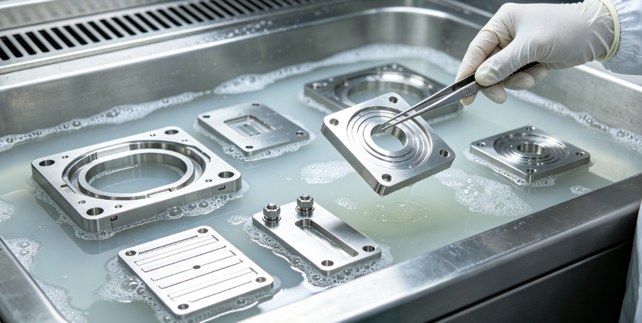
- Pre-treatment ultrasonic degreasing: Remove all machining oils, cutting fluid, and shop residue with semiconductor-grade alkaline cleaners.
- Multi-stage DI water cascade rinse: Eliminate cleaning agent residuals before passivation bath immersion
- Class 100 cleanroom citric acid passivation bath: Controlled temperature (25–40°C), calibrated dwell time tuned to part geometry and wall thickness.
- Multi-stage countercurrent ultra-pure DI rinsing (conductivity verified <1μS/cm) to strip all citric acid traces
- Low-particle nitrogen air drying inside isolated cleanroom zone — no ambient air contact to prevent dust adhesion.
- Mandatory compliance testing: Copper sulfate free iron test, humidity corrosion test, surface extractable metal screening.
- Dust-free sealed packaging, full test documentation included for fab audit files, express shipping to US/EU semiconductor facilities in 4–7 business days.
Exclusive Zorapid semiconductor passivation perks:
- Zero MOQ: 1-off prototype wafer fittings to mid-volume chamber component batches.
- Customized long dwell cycles for complex manifolds with deep internal channels.
- Full NDA protection for proprietary semiconductor chamber hardware designs.
- Dedicated surface treatment engineers familiar with SEMI and fab quality audit requirements.
Critical Compliance Standards
Semiconductor surface treatment lives or dies by audit-ready documentation. Our passivation process aligns with all global semiconductor manufacturing standards:
- ASTM A967-25: Full compliance with Type 4 citric acid passivation specifications, all required validation test records included per batch.
- SEMI F57: Meets strict limits for metal ion extractables, surface particulate, and organic residue for ultra-high-purity gas & fluid delivery systems.
- Class 100 Cleanroom Processing: All post-passivation rinsing, drying, and packaging completed in low-particulate controlled environments to avoid secondary contamination
- ASTM A380: Standard practice for descaling, cleaning, and surface evaluation of stainless steel process components
Every shipment ships with a full certificate of compliance listing bath parameters, dwell times, rinse conductivity results, and passivation validation test data — ready for fab quality and regulatory audits without extra paperwork.
Passivation vs Electropolishing: When to Use Each for Semiconductor Parts
Engineers often mix up these two surface treatments for stainless steel semiconductor hardware. They serve distinct jobs, and many critical fab components require both processes in sequence.
Core Difference Breakdown
Passivation
- Primary goal: Remove free iron, build uniform anti-corrosion chromium oxide film
- Minimal material removal (nanometers of surface metal lost)
- Leaves original surface roughness unchanged
- Ideal for structural chamber frames, mounting brackets, vacuum fittings, non-wetted external hardware
- Lower cost, faster processing for mid-volume component batches
Electropolishing (EP)
- Primary goal: Electrochemically smooth micro surface peaks, achieve ultra-low Ra finish (<0.25μm)
- Removes measurable microns of surface material
- Creates a superior enriched chromium passive film as a secondary benefit
- Mandatory for wetted gas manifolds, DI water piping, wafer carrier contact surfaces (SEMI F19 requirement)Able Elect…
Zorapid Recommended Hybrid Workflow for Critical Wetted Parts
- CNC machine 316L stainless steel component
- Electropolish to SEMI-compliant low-Ra smooth finish
- Full citric acid passivation to lock in maximum anti-corrosion performance
- Cleanroom rinse, dry, package
This two-step combo eliminates both particulate trapping and corrosion risk for high-purity semiconductor fluid/gas systems. For non-wetted structural hardware, standalone passivation delivers sufficient protection at lower cost.
Real Fab Case Study: Passivation Fixed Wafer Gas Line Contamination & Corrosion
A US semiconductor equipment startup partnered with Zorapid to resolve a critical yield issue on their new ultra-high-purity nitrogen gas manifold assembly.
Their original mistake: They sourced raw CNC 316L manifolds without passivation to cut prototype lead time. After 3 weeks of fab testing, two major failures emerged:
- Micro rust pitting formed along internal weld seams, shedding iron particles into nitrogen supply lines
- Wafer probe testing showed consistent metal ion contamination, dropping production yield by 12%
Local surface finishers only offered nitric acid passivation, which the fab rejected over nitrate residue risk.
Our Zorapid cleanroom citric passivation solution:
- Ultrasonic full internal channel degreasing to remove welding heat tint and embedded iron
- Extended 75-minute citric acid passivation dwell time for complex internal manifold geometry
- 6-stage ultra-pure DI countercurrent rinsing + nitrogen cleanroom drying
- Full copper sulfate free iron testing and SEMI F57 extractable metal analysis
Project Outcomes:
- Zero surface free iron detected post-treatment, no further pitting corrosion during 60-day fab field trials
- Wafer yield contamination issue fully resolved, 12% yield loss eliminated
- Total surface treatment cost 38% lower than local electropolish-only vendor quotes
- Manifold design locked in 2 weeks ahead of schedule for pilot fab deployment
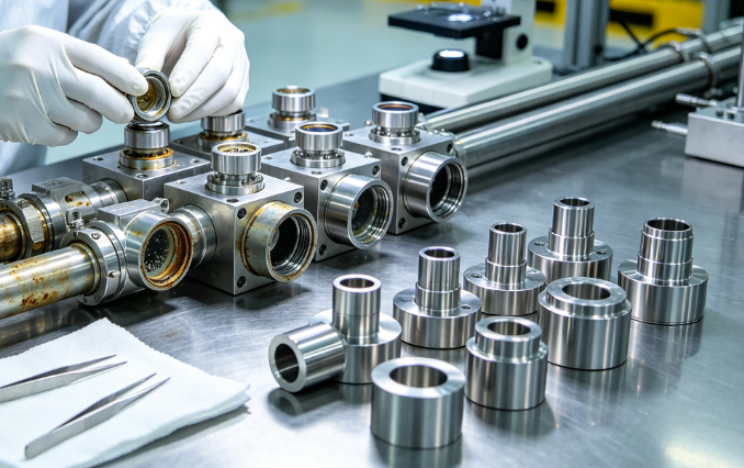
Semiconductor Stainless Steel Parts That Require Mandatory Passivation
Any stainless steel component that touches process gases, DI water, wafers, or sits inside high-humidity cleanroom chambers needs passivation. Our most common semiconductor passivation orders include:
- Ultra-high-purity gas distribution manifolds & tubing fittings
- Wafer carriers, edge grips, and handling tooling
- Vacuum chamber structural frames, flanges, and fasteners
- Wet bench fluid piping, valve bodies, and heat exchangers
- E-beam, deposition, and etch chamber internal brackets
- Cleanroom equipment enclosures and process fixture hardware
Even secondary non-wetted structural brackets benefit from passivation — ambient cleanroom humidity will slowly corrode unprotected stainless steel over long production runs.
Passivation Validation Tests We Run for Every Semiconductor Batch
We never ship semiconductor stainless steel parts without full anti-corrosion and cleanliness validation. Each lot undergoes three mandatory ASTM A967 tests:
- Copper Sulfate Free Iron Test: Confirms zero soluble iron particles on all internal and external surfaces (the primary passivation pass/fail check)
- High Humidity Corrosion Test: 48-hour controlled humidity exposure to verify no rust spot formation
- DI Water Extractable Metal Screening: Measures trace iron/chromium leaching to meet strict SEMI F57 contamination limits
Custom additional testing available upon request: salt spray testing, surface roughness Ra measurement, ESCA surface elemental analysis for chromium oxide layer verification.
FAQ
Can I skip passivation if I electropolish my semiconductor stainless steel parts?
Electropolishing creates a better passive film, but it does not replace dedicated passivation. Weld seams, threaded holes, and hidden crevices retain free iron after EP. Combined EP + citric passivation delivers full anti-corrosion and contamination control for critical wetted components.
Is citric acid passivation fully compliant with SEMI cleanroom standards?
Yes. Citric acid is chloride-free, non-toxic, leaves no nitrate residuals, and passes all SEMI F57 extractable metal limits for ultra-high-purity semiconductor process systems. It is the industry standard for modern chip fabs.
How long does passivation anti-corrosion protection last inside a semiconductor cleanroom?
Properly executed semiconductor-grade citric passivation delivers permanent corrosion resistance under standard fab operating conditions. The self-healing chromium oxide film regenerates continuously with oxygen exposure, requiring no re-treatment for the full service life of chamber hardware.
Does passivation alter part dimensions or surface roughness?
No. Citric passivation removes only atomic-level surface contaminants; measurable dimensional change is undetectable, and original surface Ra remains identical post-treatment.
Do you offer passivation for custom complex manifolds with deep blind holes and narrow internal channels?
Absolutely. We use ultrasonic pre-cleaning and extended passivation dwell cycles to ensure full uniform film coverage on hard-to-reach internal geometry, plus multi-stage countercurrent rinsing to eliminate trapped chemical residues.
What stainless steel grades do you support for semiconductor passivation?
Our primary stock is 316L and 316Ti low-carbon stainless steel — the standard alloys for semiconductor process hardware. We also handle 304 passivation for non-critical cleanroom structural enclosures.
Final Thoughts
Passivation is not an optional after-finish step for semiconductor stainless steel — it’s mandatory quality control to protect fab yield, extend equipment lifespan, and avoid costly unplanned maintenance.
Raw machined stainless steel carries hidden free iron contamination that ruins wafer production and triggers corrosion in humid, chemical-rich chip manufacturing environments. Semiconductor-grade citric acid passivation builds an invisible, self-repairing chromium oxide barrier that eliminates both risks entirely.
For critical wetted gas and fluid components, pair passivation with electropolishing to hit SEMI low-Ra surface requirements. For structural chamber hardware, standalone cleanroom passivation delivers reliable long-term anti-corrosion performance at a lower project cost.
At Zorapid, our dedicated Class 100 passivation lines are built exclusively for semiconductor OEMs, equipment startups, and fab engineering teams. We eliminate guesswork around compliance, chemical selection, and complex manifold surface treatment.
Get Your Cleanroom-Grade Passivation DFM Review & Quote Today
Upload your stainless steel part drawings or CAD files to our secure RFQ portal. Zorapid’s semiconductor surface treatment engineers will deliver a transparent, no-obligation quote within 24 hours, including clear recommendations for standalone passivation or hybrid electropolish + passivation workflows, plus free DFM feedback to optimize rinsing and surface uniformity for complex chamber geometry.
Whether you need a single prototype wafer fitting or mid-volume batches of production manifold hardware, we deliver fully ASTM/SEMI compliant passivated stainless steel parts with complete audit-ready test documentation and zero hidden processing fees.