The semiconductor industry has evolved continuously over the past few decades and serves as the driving force behind innovation and modern electronic products. This sector is committed to meeting the growing demand for efficient, compact, and durable components. CNC machining plays a vital role in manufacturing these parts with nanometer-level precision and accuracy.
It is crucial to present clear and straightforward explanations. This article covers all essential details of precision CNC machining for semiconductors, highlighting its importance, role in modern technology, and existing challenges.
Understanding Semiconductor Manufacturing
Semiconductor manufacturing involves complex processes to fabricate integrated circuits with transistors on silicon wafers. Through doping, etching, and photolithography, electronic chips for various industries are ultimately produced.
What Is a Semiconductor and Why Is It So Important?
Semiconductor materials are the foundation of modern electronic products. They are widely applied in smartphones, automobiles, computers, aerospace and many other fields. They are used to manufacture a full range of electronic devices, from simple diodes to complex electronic circuits.
What Machines Are Used in Semiconductor Manufacturing?
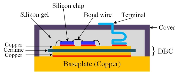
CNC machines (including CNC mills, CNC lathes, cutting machines, and less common plasma cutters and laser cutters) are widely used in semiconductor electronic processing. They deliver nano-precision cutting and shaping for wafers and related components. For wafer fabrication and IC production, CNC equipment such as dicing machines are adopted for wafer cutting, alongside specialized machines for grinding, polishing and etching processes.
Role of Semiconductor Manufacturing Technicians
Semiconductor manufacturing technicians are skilled professionals specialized in operating, maintaining, and troubleshooting complex production machinery. They ensure manufactured microchips and other components meet the stringent standards required for high-performance electronic devices. Their responsibilities also cover quality control, cleanroom environment management, and equipment fault diagnosis and troubleshooting.
Semiconductor CNC Machining Technology
CNC machining plays a vital role in semiconductor manufacturing. It accurately shapes and forms high-precision, high‑functionality components, heat sinks, and housings.
Why CNC Machining Is Critical for the Semiconductor Industry
CNC precision machining enables the accurate fabrication of complex semiconductor wafers, which is essential for high performance and functionality. It also produces identical parts with consistency and uniformity, and supports automation in electronic processing. CNC machining is a cost‑effective process customized for semiconductor material applications.
What Are the 3 Main Types of Machining Technologies?
There are three primary categories of machining technologies:
CNC Turning
Produces cylindrical parts by rotating the workpiece against a fixed cutting tool.
CNC Milling
Creates complex shapes using multi-tooth rotating cutters. It removes material from the workpiece and can form a wide variety of profiles and features.
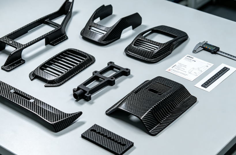
Custom CNC Machining
Best suited for prototypes, one‑off components, or discontinued parts. Common machines include 3‑axis, 4‑axis, and 5‑axis milling machines, lathes, or mill‑turn centers.
Advanced Machining Capabilities for the Semiconductor Industry
Advanced electronic manufacturing capabilities include:
Etching and Photolithography
Photolithography transfers patterns from a photomask to photosensitive material on semiconductor wafers. Common types include optical lithography and electron‑beam lithography. Advanced techniques include Extreme Ultraviolet (EUV) lithography and multi‑patterning.
Etching selectively removes material from wafers to create desired patterns. Common types are wet etching and dry etching, which are critical for forming complex 3D structures and interconnects inside semiconductor devices.
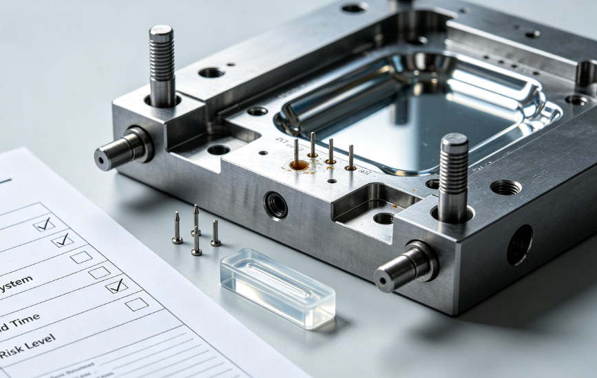
CAD/CAM Integration
CAD/CAM integration streamlines design and manufacturing workflows, enabling high‑precision input and efficient production of complex circuits, such as those used in 3D printing.
API-Enabled Machinery
API‑enabled machinery allows communication and data exchange between software and equipment in the semiconductor industry, supporting automation, data collection, and equipment control. It is essential for the advancement of Semiconductor Industry 4.0.
Innovations in Multi‑Axis CNC Machining
Innovations such as 3D printing in the semiconductor industry focus on high precision, automation, and sustainability. They deliver complex, high‑quality parts while reducing waste and downtime.
Example Applications of Semiconductor Machining
Electronic applications include Aluminum Nitride (AlN) products, known for electrical insulation and thermal conductivity, used in heat dissipation devices, LED lighting, heat sinks, substrates, and packaging for high‑power and high‑frequency electronics. Other industrial uses include molten material handling, medical equipment such as MRI systems, and microwave device packaging.
Another semiconductor material, Silicon Nitride, is used in high‑stress and high‑temperature applications such as cutting tools, automotive engine components, bearings, and biomedical implants.
The Role of Machine Shops in Semiconductor Manufacturing
Machine shops equipped with CNC machines play a vital role in manufacturing high-precision components such as heat sinks, wafer carriers, and enclosures.
Advantages of CNC Machining for Semiconductor Parts
CNC machine tools for semiconductor materials offer numerous benefits:
- Produces high-precision complex components with minimal tolerance errors.
- Delivers superior surface finish for semiconductor parts via precision CNC machining.
- Streamlines production with faster turnaround and shorter lead times.
- Highly flexible and easily programmable to accommodate design modifications.
- Cost-effective, minimizing material waste and labor costs.
- Ensures consistent accuracy and precision of parts for higher quality and reliability.
- Highly automated processes greatly reduce human error.
CNC Machining Real-World Case Studies
Case studies of practical CNC machining applications, highlighting its flexibility and precision across various industries:
Medical Devices
CNC machining produces small, complex, and polished components for medical equipment such as surgical devices.
Aerospace Parts
Aircraft parts are manufactured with high precision and accuracy, complying with strict industry standards such as AS9100 Rev D.
Petroleum Industry Measuring Equipment
Production of tank measuring equipment critical to the oil and gas industry.
5-Axis Machining Centers
BAW has secured a niche market with its 5-axis machining centers, saving 50 minutes per working hour and increasing productivity by over 60%.
How Much Does Semiconductor Equipment Cost?
The cost analysis of semiconductor equipment involves machine type, material costs, labor, installation expenses, lead time, and part complexity—all of which impact the total project cost.
Costs for major machining processes can range from $50,000 to $100,000, with some exceeding $10 billion.
State-of-the-art photolithography machines from ASML cost approximately $40 billion.
Challenges in Semiconductor CNC Machining
Below are some common challenges encountered during semiconductor CNC machining:
Thermal Expansion and Contraction
During manufacturing and packaging, semiconductor materials undergo thermal expansion and contraction due to temperature fluctuations. This induces internal stress, cracks, and long-term reliability issues.
Machining of Thin-Walled Parts
Thin-walled component machining faces inherent difficulties including low structural rigidity, complex thermo-mechanical coupling, weak damping performance, and time-varying dynamic characteristics. These factors greatly increase the difficulty of high-precision semiconductor manufacturing.
Resolving Material Strength and Impact Resistance Issues
A major challenge lies in the machinability of semiconductor materials. Materials such as silicon and quartz are often difficult to process; they tend to harden, become brittle, or deform under high temperature and pressure. Excessive heat and friction during machining can also damage or distort semiconductor components.
Tips to Optimize CNC Machining Performance
To optimize CNC machining operations for semiconductors:
Adopt designs with minimal tight tolerance requirements, avoid overly thin walls and miniature features, use industry-standard hole sizes, add fillet radii to internal edges, select suitable raw materials, and deploy optimal cutting tools as well as experienced operators.
Precision CNC Machining for the Semiconductor Industry
Tips for Achieving Precision Machining Results
Achieving High-Tolerance Machining for Semiconductor Parts
Micron-level tolerance results can be achieved through proper material selection, high-quality tooling, cleanroom environments, strict quality control measures, and CNC machine capabilities that comply with industry standards.
Impact Resistance and Structural Strength of Materials
The effects of mechanical force and impact during machining can be minimized by adopting optimal geometries, profiles, and dimensions, as well as designs that distribute stress evenly. Another key factor is selecting the appropriate impact force and cutting speed to regulate material mechanical response.
Material Preprocessing and Surface Treatment
To ensure optimal machining performance for semiconductors, silicon needs to be processed into high-purity monocrystalline wafers via cleaning, polishing, and doping. Surface treatments such as etching, deposition, and plasma processing can further enhance properties like higher yield efficiency and lower defect rates.
High-Precision Machined Components for Flexible Electronics
These components play a critical role in flexible electronic circuits. They enable the production of complex parts with micron-level tolerances, which are essential for high equipment performance and reliability.
CNC-based processes including micromachining, laser machining, EDM, and Swiss-style machining are widely used to fabricate high-precision electronic circuits.
Applications and Examples of CNC Machining in the Semiconductor Industry
CNC Machining for Wafer Fabrication and IC Production
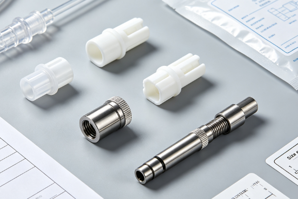
CNC machines are used not only for wafer production and IC manufacturing, but also for making fixtures and tools that handle and process wafers, ensuring precise alignment and placement. Other components produced include heat sinks, semiconductor enclosures, connectors and terminals, as well as specialized equipment for custom wafer and IC production.
CNC Solutions for Custom Semiconductor Components
Semiconductor parts such as distro plates made of ultra-pure silicon carbide ensure uniform gas flow. They feature high thermal conductivity, low impurity levels, and corrosion resistance during wafer processing. CNC machines are used to cut and shape them to the required form, with nano-precision holes for water block connections.
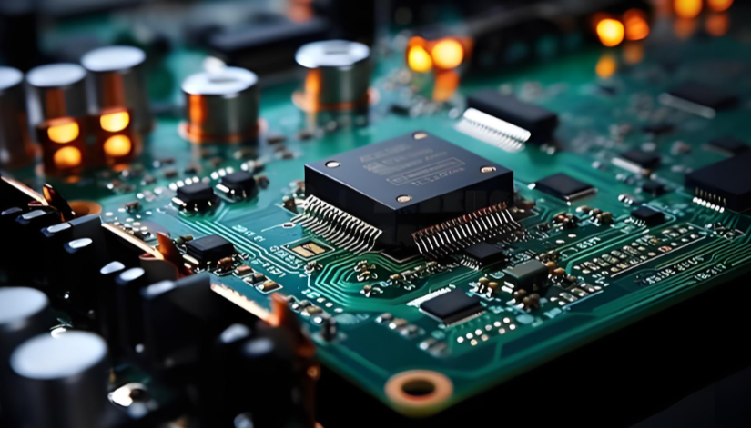
Electronic Circuits and High-Tech Manufacturing
CNC milling and turning can create custom high-precision printed circuit boards (PCBs). They remove copper from substrates and create complex paths and cuts for sophisticated circuits. As an advanced alternative to traditional etching, this process is safer and chemical-free.
The Importance of Surface Finish in Semiconductor CNC Machining
Precise surface finish is critical to the performance, functionality, and durability of semiconductor components. It affects key factors such as electrical conductivity, optical properties, and heat dissipation.
What Kind of Surface Treatment Do Semiconductors Require?
Semiconductors demand extremely flat, highly polished surfaces or mirror-grade finish. This enables consistent, nanometer-level precise device functions for silicon and sapphire substrates. It also supports accurate alignment and the formation of complex internal structures within semiconductor devices.
The Role of Custom Machining in Surface Finish Optimization
Custom machining directly impacts surface finish optimization. It can control the roughness and overall quality of custom parts by regulating cutting speed, feed rate, tool wear, and tool geometry.
How Zorapid Can Help
Zorapid provides custom CNC machining services, offering end-to-end solutions from prototype development to mass production. We prioritize quality, innovation, and customer satisfaction above all else. Our custom services are design-driven, and our experienced engineers will analyze requirements and manufacture parts that fully meet your needs.
FAQ
What are the special requirements for semiconductor CNC machining?
Strict dimensional & geometric tolerances, burr-free ultra-clean surfaces, high flatness for vacuum sealing, low-outgassing materials, oil-free processing and cleanroom assembly compliance.
What materials are commonly used for semiconductor parts?
6061/7075 aluminum, 304/316L stainless steel, titanium alloy, anodized aluminum, PEEK, PPS and other low-outgassing, corrosion-resistant engineering materials.
What precision is required for semiconductor machining?
Standard tolerance ±0.01~±0.02mm; critical sealing and mating features up to ±0.005mm with extremely strict flatness, parallelism and positional tolerance.
What are Zorapid’s advantages in semiconductor CNC machining?
Zorapid specializes in semiconductor precision components with 1-piece prototype to small-batch production. We control burr cleanliness, vacuum flatness and GD&T tolerances, providing compliant anodizing, passivation and high-purity finishing.