Published:Zorapid.Ltd
Semiconductor wafer test fixtures are critical hardware that securely holds, positions, and electrically contacts silicon wafers during probing, parametric testing, and final validation. These fixtures demand ultra-tight dimensional accuracy, precise flatness, controlled dielectric properties, low particle generation, and high chemical compatibility with cleaning solvents and wafer processing chemicals. Traditional manufacturing methods—CNC machining of PEEK, FR4, or ceramic—often face long lead times, high tooling costs, complex micro-feature limitations, and slow iteration cycles.
SLA (Stereolithography) 3D printing uses UV-curable photopolymer resins and high-precision laser curing to directly build high-resolution, complex custom wafer test fixtures. This blog covers core benefits, key SLA resin selection, design guidelines, process best practices, validation standards, limitations, and real-world applications for semiconductor wafer test fixture manufacturing.
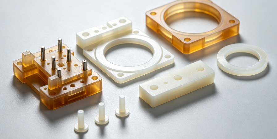
Why SLA Is the Preferred Process for Semiconductor Wafer Test Fixtures
Wafer testing environments impose extremely strict requirements: zero particle generation, zero wafer scratching, precise micro-gap positioning, stable ESD protection, and long-term dimensional stability. Traditional manufacturing methods struggle to satisfy all conditions simultaneously, while industrial SLA solves most pain points in one process.
Superior Precision & Isotropic Dimensional Stability
SLA uses a focused UV laser (405nm industrial wavelength) to cure liquid photopolymer resin layer by layer. With layer heights ranging from 25μm to 50μm and laser precision up to ±0.02mm, SLA produces fully isotropic parts with no layer stepping, no vertical anisotropic error, and consistent accuracy across XY and Z axes. This is essential for wafer micro-slot positioning, probe needle clearance trenches, tiny vacuum hole arrays, and ultra-thin wafer support ledges.
Ultra-Smooth Surface Eliminates Wafer Damage Risk
Wafer surfaces feature fragile photoresist layers, metal circuitry, and dielectric coatings. Even minor tool marks, burrs, or rough textures can cause wafer scratching, die cracking, or micro-particle contamination. Industrial SLA delivers as-printed Ra 0.4–0.8μm surface finish, which can be further polished to Ra ≤0.2μm—mirror-level smoothness that guarantees safe contact with bare wafers, dies, and thin-film surfaces.
Tunable ESD Static Dissipation for Chip Protection
Semiconductor bare dies and advanced-node wafers are extremely sensitive to electrostatic discharge (ESD). Standard plastic and most 3D-printed materials are either fully insulating (static buildup) or overly conductive (short-circuit risk). Specialty SLA ESD resins maintain acontrolled surface resistivity of 10⁶–10⁹ Ω/sq, providing gradual, uniform static dissipation without current leakage. This matches SEMI cleanroom ESD standards for wafer handling and probing stations.
Ultra-Low Outgassing & Zero Dust Generation
Industrial semiconductor-grade SLA resins are formulated with low-volatility monomers, zero-filler precipitation, and fully cross-linked curing structures. They produce negligible outgassing, no powder shedding, and no micro-particle debris after full post-cure—critical for Class 100 / ISO 7 cleanroom wafer test environments.
Fast Iteration & Low Cost for High-Mix Semiconductor R&D
Wafer probe layouts, pitch sizes, cavity depths, and vacuum patterns change frequently for new wafer tape-outs, process node upgrades, and package variations. CNC machining requires days for revision and high custom tooling fees. SLA printing completes full fixture iteration within 4–12 hours, enabling engineers to validate probe clearance, wafer flatness support, and optical alignment structures overnight.
Industrial SLA Resin Material Grades for Wafer Test Fixtures
Consumer-grade general resin is not acceptable for semiconductor tooling. Only industrial low-shrink, low-outgassing, ESD-stable, and cleanroom-certified photopolymers qualify for wafer test applications.
ESD Black Low-Shrink Resin (Most Widely Used)
Core application: Wafer carrier trays, probe station base jigs, die positioning fixtures, vacuum chuck auxiliary tools, test socket supports
Key properties:
- Surface resistivity: 10⁶–10⁹ Ω/sq (stable under humidity fluctuation)
- Cure shrinkage: <0.2% (minimal long-term warpage)
- Zero powder shedding, low outgassing, fully cross-linked rigid structure
- High hardness and wear resistance for repeated wafer loading/unloading cycles
High-Transparent Optical Grade SLA Resin
Core application: Vision alignment fixtures, top-view probe inspection jigs, optical calibration frames, wafer backside inspection supports
Advantages: Uniform light transmittance, no internal scattering spots, stable optical clarity under long-term UV and cleanroom lighting, compatible with machine vision positioning algorithms.
High-Temperature Rigid Resin
Core application: Thermal wafer test fixtures, high-temperature probe station jigs, bake-process auxiliary tooling
Features: Heat deflection temperature (HDT) >80°C, minimal thermal expansion, no softening or deformation during thermal cycling tests.
Low-Stress Tough Resin
Core application: Thin-walled flexible supports, ultra-thin wafer edge protection frames, repeatedly clamped fixtures
Features: Anti-brittle fracture, high fracture toughness, resistance to micro-cracking under cyclic mechanical stress.
Standard SLA Printing Process for Semiconductor-Grade Fixtures
Semiconductor SLA tooling requires a strict cleanroom-oriented SOP—different from ordinary prototype printing. Every step targets zero contamination and maximum dimensional stability.
Pre-Print DFM & Compensation Design
- Uniform wall thickness design to avoid uneven curing stress
- Precision shrinkage compensation mapping for micro holes, gaps, and positioning bosses
- Support placement limited to non-contact non-critical surfaces
- Eliminate sharp corners to prevent micro-stress concentration and post-cure warpage
High-Precision Layered Printing
Adopt 25–50μm ultra-fine layer height with closed-loop laser power calibration. Uniform laser energy density ensures consistent curing depth, avoiding incomplete curing or over-cured brittleness. All critical wafer contact surfaces are printed with optimized laser scanning paths to eliminate micro-waviness.
Strict IPA Cleaning & Residue Removal
After printing, parts undergo multi-cycle IPA immersion and ultrasonic cleaning to completely remove residual liquid resin on micro-trenches, hole arrays, and gap structures. Residual resin is the main cause of particle contamination and wafer staining in cleanroom environments.
Secondary Uniform UV Post-Curing
Semiconductor fixtures require extended, uniform post-curing to achieve full cross-linking. This step stabilizes mechanical properties, eliminates latent shrinkage, reduces outgassing, and ensures long-term dimensional stability in cleanroom environments.
Micro-Polishing & Cleanroom Finishing
Wafer contact surfaces are finely polished to eliminate tiny layer lines. All edges are chamfered and deburred to prevent wafer edge chipping. The final finished surface achieves mirror-level smoothness with no sharp micro-edges.
Dimensional Metrology & ESD Batch Testing
Every batch fixture undergoes full inspection: optical dimension scanning, key tolerance verification, flatness detection, and surface resistivity testing. Only parts meeting SEMI ESD standards and dimensional Cpk ≥1.33 are released for cleanroom use.
Dust-Free Vacuum Packaging
Finished fixtures are ultrasonically cleaned, nitrogen blow-dried, and sealed in Class 100 cleanroom packaging to prevent secondary particle contamination during transportation and storage.
Tolerance & Surface Finish Industry Benchmarks
Semiconductor wafer test fixtures have stricter tolerance standards than general industrial jigs.
- Critical positioning features: ±0.02mm ~ ±0.03mm
- General structural dimensions: ±0.05mm
- Flatness of wafer contact plane: ≤0.03mm
- Surface roughness (wafer contact area): Ra ≤0.2–0.4μm
- ESD resistivity stability: 10⁶–10⁹ Ω/sq (constant under 30–60% RH humidity)
- Particle level: Zero visible micro-particles under 10× magnification
Core DFM Design Rules for Wafer Test SLA Fixtures
Avoid Local Over-Thick & Over-Thin Transition
Abrupt thickness differences cause inconsistent curing speed and residual stress, leading to long-term warpage and flatness deviation. Maintain gradual transition fillets and uniform wall thickness for all contact platforms.
Isolate Probe Clearance Zones from Wafer Support Zones
Probe needle moving gaps require ultra-smooth vertical walls and precise dimensional control; wafer bearing surfaces require perfect flatness. Separating functional zones avoids mutual interference during printing and post-processing.
Optimize Vacuum Hole & Micro-Pore Layout
Vacuum suction holes for wafer fixing must maintain consistent aperture size and no burrs. SLA printing enables uniform micro-hole arrays that CNC cannot easily achieve, ensuring balanced wafer suction and preventing wafer warping during testing.
No Sharp Corners on Wafer Edge Contact Areas
All wafer edge contact positions must adopt rounded transitions to prevent edge chipping and thin-wafer cracking during repeated loading.
Failure Analysis & Industry Common Defect Solutions
Long-Term Warpage & Flatness Drift
Causes: Insufficient post-curing, uneven wall thickness, low-grade high-shrinkage resin, unstable printing temperature
Solutions: Use low-shrinkage semiconductor resin, extend uniform UV curing, apply structural DFM optimization, and implement temperature-constant printing environment
Unstable ESD Resistance
Causes: Non-semiconductor-grade conductive filler resin, incomplete curing, humidity interference
Solutions: Adopt professional ESD photopolymer formula, batch resistivity testing, and humidity-stabilized cleanroom storage
Wafer Micro-Scratch & Particle Contamination
Causes: Residual uncured resin, insufficient polishing, non-cleanroom post-processing environment
Solutions: Multi-stage ultrasonic cleaning, mirror polishing, full cleanroom finishing and packaging
Micro-Hole Blockage & Uneven Vacuum Suction
Causes: Printing residue accumulation, incomplete cleaning
Solutions: Optimize slicing path for micro-holes, high-pressure nitrogen cleaning, and final microscopic inspection
SLA vs CNC vs FDM for Wafer Test Fixtures (Full Comparison)
| Performance Item | SLA Resin Printing | CNC Machining | FDM Printing |
|---|---|---|---|
| Dimensional Accuracy | ±0.02–0.05mm (Excellent) | ±0.02mm (Excellent) | ±0.1–0.2mm (Poor) |
| Surface Smoothness | Mirror finish Ra 0.2–0.4μm | Smooth but tool-mark residual | Obvious layer lines |
| ESD Stability | Controllable 10⁶–10⁹Ω | Metal conductive risk / plastic unstable | No stable ESD grade |
| Particle Contamination Risk | Ultra-low | Tool dust risk | High shedding risk |
| Complex Micro Structure Ability | Perfect (micro slots, hole arrays) | Limited by tool diameter | Unable |
| Iteration Speed | Ultra-fast (hours) | Slow (days) | Fast but low quality |
| Unit Cost (Custom Fixture) | Low–Medium | High | Low (not qualified) |
Production Qualification & Cleanroom Compliance Standards
Qualified SLA wafer test fixtures must comply with semiconductor industrial specifications:
- SEMI ESD S20.20 electrostatic protection standard
- ISO 7 / Class 100 cleanroom particle control requirements
- Low outgassing & low volatile residue certification
- Full batch traceability: resin lot, printing parameters, curing records, inspection logs
- Long-term aging stability test (72h high-temperature & humidity cycling)
Typical Mass-Production Application Scenarios
- 8-inch / 12-inch wafer probing station positioning fixtures
- Wafer vacuum carrier trays and edge protection jigs
- Die sort test fixtures and micro-chip positioning holders
- Optical wafer inspection & AOI alignment tooling
- Probe needle clearance isolation frames
- Semiconductor thermal cycling test auxiliary jigs
Final Summary
SLA resin 3D printing has evolved from a simple prototyping method into a high-reliability, cleanroom-qualified industrial manufacturing process for semiconductor wafer test fixtures. Its unique advantages in micro precision, mirror surface quality, controllable ESD performance, ultra-low contamination, and rapid iteration perfectly match the high standards of wafer CP testing, FT testing, and die sorting processes.
For semiconductor R&D and mass-production test tooling, industrial SLA is no longer an alternative solution—it has become the most balanced, cost-effective, and high-yield standard process for custom micro-precision wafer fixtures.