Published:Zorapid.Ltd
Semiconductor R&D teams rely on tiny precision prototypes daily: wafer holding nests, probe socket housings, microfluidic test carriers, optical alignment jigs, and low-outgassing lab fixtures. Two manufacturing methods dominate early-stage validation:
- High-Resolution SLA 3D Printing: UV resin additive manufacturing, optimized for ultra-fine micro features and complex internal geometry, no custom fixturing or tooling.
- Micro Precision CNC (Micro Milling / Swiss Turning): Subtractive machining of solid engineering bar stock, delivering tight micron tolerances and industrial-grade cleanroom polymer/metal materials.
Most semiconductor engineers only compare upfront per-part pricing, ignoring hidden costs: post-finishing, rework scrap, compliance documentation, thermal stability failures, and repeat iteration overhead. This review quantifies full landed cost across batch sizes, plus technical tradeoffs that directly impact fab testing yield and R&D budget waste.
All data targets low-volume semiconductor NPI batches (1–50 prototypes), the standard volume for wafer lab validation, probe station trials, and process proof-of-concept builds.
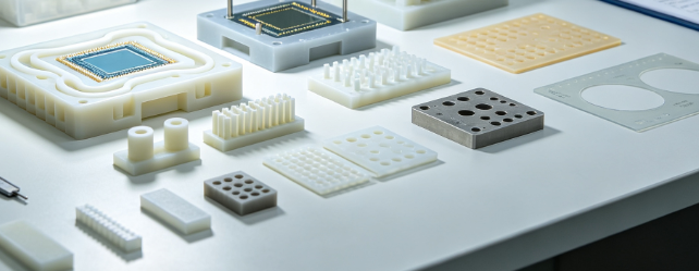
Core Semiconductor Prototype Requirements That Shape Cost & Process Choice
Semiconductor fixtures carry unique non-negotiable specs that change total manufacturing cost vs general consumer prototypes:
- Ultra-fine micro features (0.2–1mm channels, alignment pins, micro slot cutouts)
- Strict low-outgassing, low-particle cleanroom compatibility (Class 100/1000 fab environments)
- Dimensional stability under thermal cycling (chamber bake, cryo cooling, wafer processing heat swings)
- Minimal surface micro burrs to prevent silicon wafer scratch and circuit contamination
- Traceable material COA, surface roughness test logs, and full FAIR documentation for audit trails
- Frequent design iterations (3–8 revision cycles typical for new test socket hardware)
These requirements create critical cost gaps between SLA and micro CNC that generic prototype cost guides ignore.
Full Cost Breakdown: SLA vs Micro CNC for Semiconductor Small Batches
All pricing reflects semiconductor-grade cleanroom processing, not standard consumer prototyping service rates. Costs split into fixed upfront fees, variable per-unit charges, and hidden post-processing overhead.
Fixed Upfront Cost Comparison (One-Time Per Design Revision)
Fixed costs hit hardest on 1–10 piece prototype batches, the most common semiconductor R&D order size.
- SLA 3D Print Fixed Costs
- Zero CAM programming / fixture setup labor
- Minimal prep cost: CAD slice simulation + support generation ($30–$80 one-time per design)
- No custom holding jigs, zero tooling investment
- Design change cost: Only re-slice CAD ($20–$50 per revision)
- Micro CNC Fixed Costs
- CAM programming + zero-point fixture setup labor ($250–$600 per unique part geometry)
- Custom micro end mill tool purchase surcharge for <0.5mm micro features ($100–$300)
- Design change cost: Full CAM rework + fixture re-alignment ($150–$400 per revision)
- Cost Gap Takeaway: For frequent design iterations, SLA cuts fixed revision overhead by 70–85% per CAD tweak.
Variable Per-Unit Production Cost Tiers (Semiconductor-Grade Finished Parts)
Costs include base manufacturing + standard cleanroom washing; excludes specialty coating/metallization.
- Batch 1–10 pcs (R&D single iteration prototypes)
- SLA (low-outgassing semicon resin): $45–$95 / unit
- Micro CNC (PEEK / Ultem / aluminum): $180–$320 / unit
- Gap: Micro CNC is 3–4x more expensive per piece for tiny low-volume runs
- Batch 10–50 pcs (Pilot lab validation batches)
- SLA: $32–$68 / unit (volume discount for nested printing)
- Micro CNC: $110–$210 / unit (setup labor spread across more parts)
- Gap: Micro CNC still 2.5–3x higher unit cost
- Batch 50+ pcs (Limited pre-production test fixtures)
- SLA: $28–$52 / unit
- Micro CNC: $85–$145 / unit
- Break-even note: No volume threshold where micro CNC becomes cheaper than SLA for pure resin plastic geometry below 200 units
Hidden Post-Processing & Compliance Hidden Costs
These unplanned fees often add 20–40% to total prototype spend, and differ drastically between processes:
SLA Hidden Costs
- Advanced low-outgassing resin upgrade: +$12–$28 per unit (standard resin outgasses too high for fabs)
- Support mark polishing for optical alignment surfaces: +$8–$18 per unit
- Batch solvent ultrasonic cleanroom washing: Flat $70–$120 per order
- Limitation add-on: Metallization coating (EMI shielding) requires secondary plating vendor lead time surcharge
Micro CNC Hidden Costs
- Micro deburring + ultrasonic particle removal: +$30–$70 per unit (critical to avoid wafer scratch defects)
- Specialty material surcharge (medical/semicon PEEK, non-magnetic brass): +$40–$90 per unit raw stock premium
- CMM full dimensional scanning + FAIR report generation: Flat $180–$350 per batch
- Thermal stress relief for thin-wall micro frames: +$25–$50 per unit to prevent post-machining warpage
Technical Performance Tradeoffs That Impact Long-Term Semiconductor Spend
Lower upfront SLA cost can lead to higher total lifecycle spend if parts fail thermal/cleanroom testing; micro CNC carries higher upfront cost but eliminates rework scrap for high-stakes fab hardware.
Tolerance & Dimensional Stability
- SLA Semiconductor Grade: ±0.08–0.15mm baseline tolerance; severe thermal expansion drift above 80°C bake cycles. Micro alignment pins drift after repeated thermal cycling, requiring rework replacement.
- Micro CNC: ±0.003–0.015mm consistent micron tolerance; solid bar stock maintains stable dimensions across -40°C to 150°C semiconductor chamber operating ranges, zero post-processing warpage. Cost Impact: SLA prototypes for high-temperature test stations often require 2–3 reprint batches due to dimensional drift, doubling total small-batch spend.
Material Options for Cleanroom / Low-Outgassing Semicon Use
- SLA Limitations: Restricted to UV-curable photopolymer resins. Only specialty semicon-certified low-outgassing resins meet fab specs; no metal, PEEK, Ultem, or conductive shielding stock options.
- Micro CNC Material Range: Full semiconductor material portfolio: non-magnetic aluminum, 316L stainless, brass terminals, PEEK, Ultem PEI, glass-filled PC, conductive copper shielding bars. Cost Impact: If your prototype requires metal grounding, high-temp PEEK, or EMI shielding, SLA forces expensive secondary plating/assembly labor, erasing initial printing cost savings.
Micro Feature & Complex Internal Geometry Capability
- SLA Strength: Zero cost penalty for conformal cooling channels, nested microfluidic passages, blind undercuts, and organic lattice structures impossible to reach with micro end mills. Complex geometry does not raise unit price.
- Micro CNC Limitation: Deep internal micro channels require multi-setup 5-axis machining, adding $60–$120 per unit surcharge for hard-to-reach internal features. Tiny 0.2mm thin ribs risk deflection during cutting, raising scrap rates. Cost Impact: Highly complex microfluidic carriers cost 60–75% less via SLA vs micro CNC for small batches.
Thermal, Chemical & Particle Contamination Risk
- SLA Weakness: Standard resin absorbs process chemicals; surface degrades under repeated plasma/ solvent cleaning cycles, shedding micro particles into wafer processing chambers. Limited repeated lab cycle life (20–50 test runs before replacement).
- Micro CNC Strength: Solid polymer/metal stock resists solvent, plasma, and thermal cycling; polished machined surfaces generate zero loose micro particles, passing Class 100 cleanroom particle audit tests for thousands of test cycles. Cost Impact: SLA disposable single-test prototypes create recurring reorder costs; micro CNC fixtures are reusable long-term, cutting annual R&D replacement spend.
Best Use Case Matching: When to Pick SLA, When Micro CNC Is Mandatory
Choose SLA 3D Print to Minimize Total Prototype Cost If All Apply
- Batch size 1–30 units, frequent CAD design revisions (3+ iterations planned)
- Part contains complex internal microfluidic channels, deep undercuts, or lattice lightweight structures
- Operating temperature <60°C, short-term lab fit validation only (no long-duration thermal bake cycles)
- Material requirement = low-outgassing UV resin, no metal/PEEK/conductive shielding needed
- Disposable single-test hardware, no requirement for thousands of repeated fab cycles
Choose Micro CNC Even At Higher Upfront Cost If Any Single Condition Applies
- Critical micron alignment tolerances (±0.02mm or tighter) for probe socket pin positioning
- Continuous thermal cycling above 80°C (wafer bake, high-temperature process chambers)
- Requires PEEK, Ultem, non-magnetic metal, conductive copper/brass shielding components
- Hardware will be reused for hundreds/thousands of fab test cycles (long-term reusable fixtures)
- Zero particle contamination mandate for advanced node silicon wafer processing
Real Semiconductor Client Cost Case: Wafer Test Socket Prototype Batch
A US semiconductor test equipment OEM needed 8 micro socket housing prototypes for NPI probe station validation, with 3 planned design revisions.
Initial Sourcing Option 1: Micro CNC PEEK Machining
- Fixed setup/CAM cost: $420 one-time
- Per-unit price: $240 × 8 = $1,920
- Revision rework cost (3 CAD changes): $280 × 3 = $840
- Cleanroom deburr + CMM FAIR batch fee: $260
- Total landed cost for full iteration cycle: $3,440
- Additional note: Parts stable for thermal testing, no rework scrap after lab validation
Initial Sourcing Option 2: Low-Outgassing SLA Semicon Resin
- Fixed CAD slice/support prep cost: $65 one-time
- Per-unit price: $72 × 8 = $576
- Revision reprint cost (3 CAD changes): $40 × 3 = $120
- Cleanroom polishing + washing batch fee: $95
- Initial printed batch total: $856
- Hidden extra cost discovered during testing: SLA resin drifted 0.12mm after thermal bake, requiring full 4th reprint batch ($520 additional)
- Final full iteration landed cost: $1,376
Final Client Outcome
For short-term room-temperature fit checks, SLA delivered 60% lower total spend. For long-duration thermal probe testing, the client switched to micro CNC PEEK to eliminate repeated reprint scrap overhead, accepting higher upfront unit cost to remove recurring rework labor delays.
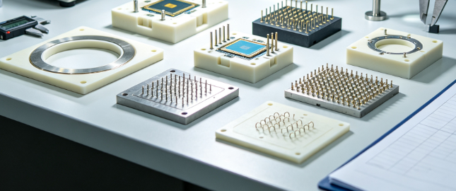
SLA vs Micro CNC Semiconductor Prototype Comparison Chart
| Evaluation Metric | High-Res SLA Semicon 3D Print | Micro Precision CNC Machining |
|---|---|---|
| Fixed One-Time Setup Cost | Very Low ($30–$80) | High ($250–$600) |
| Per-Unit Cost (1–10 pcs) | $45–$95 | $180–$320 |
| Design Revision Cost Per Change | $20–$50 | $150–$400 |
| Dimensional Tolerance Range | ±0.08–0.15mm | ±0.003–0.015mm |
| Thermal Stability (>80°C Bake) | Poor (drift risk) | Excellent, no warpage |
| Supported Materials | Only low-outgassing UV resins | PEEK, Ultem, aluminum, stainless, brass, copper |
| Complex Internal Micro Channels | No extra cost, fully feasible | High surcharge for multi-axis setup |
| Cleanroom Particle Risk | Moderate (surface degradation over cycles) | Minimal, polished solid stock |
| Typical Lead Time Per Batch | 1–3 business days | 4–8 business days |
| Best Semiconductor Batch Fit | 1–30 disposable fit-test prototypes | Reusable high-temp precision test fixtures |
| Total Lifecycle Cost (Long-Term Use) | Higher (frequent reorder scrap) | Lower (one-time purchase, thousands of test cycles) |
6 Cost Optimization Hacks for Semiconductor Prototypes (SLA + Micro CNC)
- Split prototype batches by functional requirement Use SLA for early fit iteration builds; lock finalized CAD then produce micro CNC versions for formal thermal/wafer testing to cut revision overhead.
- Standardize micro feature sizes to reduce CNC tool surcharges Adopt industry standard 0.5mm+ minimum internal radii for micro CNC parts to avoid custom micro end mill fees.
- Nest multiple small SLA parts in one single print batch Combine unrelated test carriers into one build plate to spread fixed slice/prep costs across all SKUs, cutting per-unit price by 15–25%.
- Reserve specialty low-outgassing resin only for wafer-contact surfaces Print non-critical housing sections with standard SLA resin to reduce material premium surcharges.
- Consolidate CMM inspection into one full batch report Avoid separate FAIR fees for small split prototype orders; group revisions into a single inspection run.
- Hybrid process design to balance cost and performance SLA print complex internal channel bodies, micro CNC machine only critical alignment datum surfaces to hit tight tolerances while lowering total spend.
Common Sourcing Cost Mistakes That Blow Semicon R&D Budgets
- Mistake: Select SLA purely based on low upfront quote without thermal testing data Fix: Confirm maximum operating temperature requirements; thermal drift scrap doubles total small-batch spend.
- Mistake: Ignore revision rework cost when comparing RFQs Fix: Add projected 2–4 design change fees into total landed cost comparison, not just base unit price.
- Mistake: Specify micro CNC for purely disposable fit-check prototypes Fix: Use SLA for short-term room-temperature geometry validation to eliminate expensive CAM/fixture setup labor.
- Mistake: Skip cleanroom ultrasonic deburring for micro CNC parts to save short-term cost Fix: Unremoved micro burrs scratch silicon wafers during testing, triggering costly lab test downtime and rework batches.
- Mistake: Request generic consumer-grade SLA resin instead of semiconductor low-outgassing resin Fix: Standard resin fails fab outgassing audits, requiring full reprint batches with compliant specialty resin.
FAQ
What is the break-even batch size where micro CNC matches SLA total cost?
There is no fixed volume break-even for pure resin prototypes. Micro CNC only becomes cost competitive if you require metal/PEEK materials or thousands of repeated test cycles eliminating recurring SLA replacement orders.
Can SLA printed semiconductor fixtures pass Class 100 cleanroom particle testing?
Only specialty low-outgassing semicon-certified resins qualify, and performance degrades rapidly after repeated solvent/plasma cleaning cycles. Long-term reusable fab fixtures still require micro CNC solid polymer/metal stock.
How much faster is SLA vs micro CNC for semiconductor prototype delivery?
SLA batches ship in 1–3 days; micro CNC requires 4–8 days due to CAM programming, micro tool setup, and precision CMM inspection workflows. For urgent same-week design iteration, SLA cuts lead time by 60–75%.
Can I combine SLA and micro CNC in one hybrid semiconductor fixture to balance cost and precision?
Yes. Print complex internal channel bodies via SLA, then micro machine critical alignment datum planes and mounting holes to hold micron tolerances, reducing total cost vs full micro CNC production.
Do both processes provide semiconductor-compliant FAIR and material COA documentation?
Micro CNC automatically includes full CMM scan FAIR and raw material COA as standard. SLA providers charge extra for formal dimensional audit reports unless specified upfront in the RFQ.
Wrap-Up
SLA 3D printing delivers unbeatable low upfront cost and fast iteration speed for short-term, low-temperature disposable semiconductor fit-test prototypes with complex internal microfluidic geometry. However, its thermal instability, limited material range, and short cycle life create hidden rework costs for long-duration fab testing hardware.
Micro precision CNC carries higher fixed setup and per-unit pricing for small batches, but delivers stable micron tolerances, full semiconductor-grade material compatibility, and zero particle contamination risk for reusable high-temperature wafer test sockets and alignment jigs. The higher one-time cost eliminates recurring reprint scrap and replacement spend over the full R&D validation cycle.
Zorapid offers both high-resolution semicon SLA printing and temperature-controlled micro CNC machining under one roof, enabling hybrid prototype builds to balance upfront budget and long-term testing performance. Our engineering team provides side-by-side total landed cost quotes for both processes, including projected revision and rework overhead specific to your semiconductor lab operating conditions.
Request Your Free Semiconductor Prototype Cost Comparison RFQ
Share your fixture CAD, operating temperature range, batch quantity, material requirements, and planned number of design revisions. Our semiconductor hardware team will generate itemized total landed cost breakdowns for SLA and micro CNC, plus optimized hybrid process recommendations to minimize your R&D prototype budget.