Published:Zorapid.Ltd
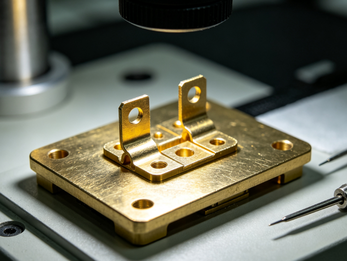
Every semiconductor test socket, probe connector, power distribution interface, and wafer stage signal connector relies on ultra-thin brass sheet metal terminals as the core conductive contact.
Aluminum and steel fail here: too high contact resistance, poor spring retention, hard to form micro bending features, and prone to oxidation that ruins high-speed signal integrity. Pure copper bends too easily and lacks mechanical elasticity for repeated mating cycles.
Brass sheet hits the perfect balance: stable electrical conductivity, excellent formability for micro stamped contact springs, natural corrosion resistance, and cost efficiency for high-volume semiconductor equipment production.
But standard commercial brass terminals won’t cut it for fabs. Semiconductor connectors demand micron-level dimensional control, burr-free cleanroom surfaces, and compliant plating to avoid particle contamination and signal loss.
This plain-language guide breaks down every detail engineers need: alloy picks, manufacturing workflows, non-negotiable DFM rules, industry plating specs, and quality standards built exclusively for semiconductor connector hardware from Zorapid’s precision sheet metal division.
Core Semiconductor Performance Demands for Connector Terminals
Semiconductor operating environments create strict non-negotiable requirements for brass sheet terminals that generic electronics terminals ignore:
- Ultra-low stable contact resistance High-speed digital signals and low-current sensing circuits cannot tolerate resistance drift from oxidized contact surfaces or rough stamped edges.
- Consistent spring retention over thousands of mating cycles Test sockets and probe connectors plug/unplug hundreds of thousands of times; terminals must maintain precise contact pressure without permanent spring fatigue.
- Zero micro burrs & particle-free surfaces Tiny metal slivers will contaminate cleanroom wafers, short PCB traces, and damage delicate silicon dies during testing.
- Tight micron dimensional tolerances Misaligned terminals cause probe offset, incomplete electrical contact, and inconsistent wafer test data. Positional tolerance down to ±0.005 mm is standard for advanced semiconductor sockets.
- Thermal stability under cycling heat loads Wafer processing equipment swings from ambient to high-temperature bake conditions; brass terminals must resist thermal expansion deformation to preserve alignment.
- Low outgassing materials & plating Outgassing residues coat optical sensors and wafer surfaces, triggering massive yield loss in fabrication fabs.
Best Brass Sheet Alloys for Semiconductor Contact Terminals
We stock semiconductor-grade cold-rolled brass sheet optimized for thin-gauge terminal forming (0.1 mm ~ 0.8 mm thickness), each alloy matched to specific connector use cases:
1. C26000 / H65 Cartridge Brass (Most Popular for Semicon Connectors)
- Copper content 65%, zinc 35%
- Balanced conductivity + spring elasticity
- Superior bending performance for thin micro contact springs
- Ideal: PCB signal connectors, low-power test socket terminals, inter-board link contacts
- Cleanroom compatibility after nickel/gold plating, minimal outgassing
2. C36000 Free-Cutting Brass
- High machinability index, clean chip removal during CNC micro cutting
- Perfect for NPI prototype terminals with complex cutouts, slots, and offset bends
- Use case: short-run R&D connector prototypes, custom probe adapter contacts
3. C26800 / H68 High Copper Brass
- Higher electrical conductivity (27~28% IACS)
- Lower resistivity for high-current power semiconductor connectors
- Less spring force than C2600; best for power distribution terminal blocks on wafer equipment
Alloy Elimination Note
Standard low-grade H62 brass is avoided for advanced semiconductor hardware: higher zinc content accelerates dezincification oxidation under thermal cycling, raising contact resistance over service life.
Zorapid’s Dual Manufacturing Routes: Rapid CNC Prototyping + High-Speed Precision Stamping
Semiconductor product development splits clearly into NPI prototype validation and mass production batches. Zorapid operates two dedicated brass sheet metal workflows to cover both stages without quality tradeoffs.
Micro CNC Sheet Metal for NPI & Low-Volume Prototypes
For 1–500 prototype terminals during connector design validation:
- Laser cut thin brass blanks with ±0.008 mm dimensional accuracy
- CNC micro press brake precision bending with springback compensation
- Ultrasonic micro deburring to eliminate all sharp edge burrs
- In-house semiconductor plating line for nickel/gold surface treatment
- Full CMM metrology inspection of every contact geometry
Key benefits for semiconductor engineers:
- No expensive progressive stamping die investment for early design iterations
- Fast CAD edits with same-day DFM feedback to tweak spring bend profiles
- Burr-free edges critical for cleanroom test equipment
- Turnaround: 3–5 business days for fully finished, ready-to-assemble brass terminals
Progressive Fine Blanking Stamping for Mass Semiconductor Batch Runs
For production volumes over 5,000 identical connector terminals:
- Custom precision progressive stamping die with multi-stage forming stations
- Fine blanking process delivers mirror-smooth vertical cut surfaces (no secondary polishing required)
- In-die bending, coining, and spring profile forming in one continuous pass
- Online inline dimensional inspection to catch drift mid-production
- Bulk batch plating with tightly controlled coating thickness uniformity
Key production advantages:
- Ultra-low per-unit cost at scale for OEM semiconductor equipment manufacturers
- Consistent spring force and dimensional repeatability across millions of terminals
- Closed dust-free stamping cell to prevent surface contamination
- Batch capacity up to millions of terminals per production run
Critical DFM Design Rules for Semiconductor Brass Terminals
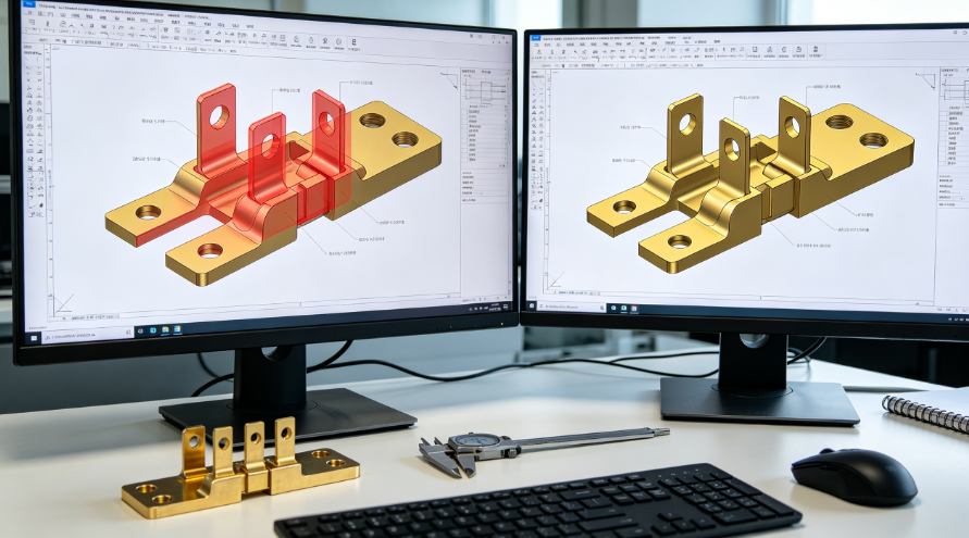
80% of terminal performance failures stem from unoptimized sheet metal geometry before manufacturing. Our semiconductor DFM engineers enforce these non-negotiable rules for brass sheet connectors:
- Minimum internal radii ≥0.05 mm on all bend and slot corners Sharp micro corners create stress cracking during repeated spring deflection, shortening connector service life.
- Maintain uniform thin sheet gauge (0.1–0.8 mm) Uneven thickness causes inconsistent spring pressure and thermal warpage under fab temperature cycles.
- Leave minimum 0.1 mm clearance between cut slots and bend lines Too-small gap creates material tearing during stamping/bending, generating contaminant micro metal flakes.
- Optimize spring arm length for controlled deflection Over-long brass spring arms deform permanently after thousands of mating cycles; DFM calculates bend force to match target contact pressure.
- Avoid blind micro recesses without deburring access Hidden trapped burrs cannot be removed and will shed particles inside cleanroom equipment.
- Compensate plating thickness in base brass dimensions Nickel + gold plating adds 2–6 μm total thickness; we offset CNC/stamping cuts to preserve final mating tolerance after finishing.
Semiconductor-Grade Plating & Surface Finishing Standards
Raw brass oxidizes rapidly, raising contact resistance and shedding zinc particles. All semiconductor brass terminals require controlled plating following SEMI cleanroom standards:
Standard Stacked Plating Layer Spec (Mating Contact Zones)
- Base underlayer: 2–3 μm electroless nickel (barrier layer to stop brass zinc diffusion)
- Contact surface: 0.05–0.15 μm hard gold plating Hard gold delivers wear resistance for 100,000+ mating cycles and ultra-stable low contact resistance.
Alternative Finishing Options
- Selective gold plating: Only plate the mating contact area to cut material cost (non-contact zones stay tin-nickel plated)
- Matte tin plating: Low-current static signal connectors, cost-effective for non-critical secondary terminals
- Passivation only: For internal non-contact structural brass brackets (no gold required)
Strict Cleanroom Plating Controls
All plating lines run in low-particle enclosed bays, with full post-plating ultrasonic solvent cleaning to remove chemical residues that cause outgassing in semiconductor fabs.
[Image Placement 4: Finished part collage – gold-plated micro brass spring terminals, tin-plated power terminal blocks, close-up polished contact surface]
Strict QA Metrology for Cleanroom-Ready Brass Terminals
Semiconductor customers require full traceable inspection reports for every batch of brass sheet terminals:
- 100% dimensional sampling via optical vision measuring machines Verify bend angle, spring arm length, slot width, pin positional tolerance down to ±0.005 mm
- Contact resistance testing Benchmark resistance values to eliminate high-resistance defective terminals before assembly
- Plating thickness XRF spectroscopy inspection Confirm nickel/gold layer thickness meets SEMI connector specs, no uneven coating
- Surface particle & burr audit under high-magnification microscope Zero micro burrs, scratches, or loose metal flakes allowed for cleanroom use
- Spring fatigue cycle testing (accelerated lab validation) Simulate 100,000 mating cycles to confirm no permanent deformation of brass contact springs
- Full material certification & batch compliance documents All brass sheet stock comes with alloy COA for semiconductor audit trails
Real Semiconductor Client Case: Wafer Test Socket Brass Terminals
A semiconductor probe equipment OEM needed thin C26000 brass sheet terminals for 300 mm wafer test sockets, 200 prototype units followed by 50,000 production parts.
Original Design Pain Points
- Sharp internal slot corners caused spring cracking during repeated probe contact
- Uncompensated bend springback led to inconsistent contact pressure across the socket
- Uncontrolled plating thickness threw off tight pin alignment tolerances
- Rough stamped edges generated micro metal particles that scratched silicon wafers during testing
Zorapid Brass Sheet Metal Solution
- DFM redesign added 0.06 mm internal radii on all cut slots to eliminate stress fracture
- CNC bend springback compensation calibrated for C26000 brass alloy to lock uniform contact force
- Pre-plating dimensional offset on all critical mating features to account for nickel-gold coating thickness
- Fine blanking + ultrasonic micro deburring delivered burr-free, particle-safe contact surfaces
- Dual workflow delivery: Micro CNC rapid prototypes shipped in 4 days; progressive stamping mass batch completed in 12 days
Final Outcome
Zero wafer scratch incidents during client lab validation, consistent low signal resistance across all sockets, scrap rate dropped from 28% to under 1.2%. The OEM now sources all brass connector terminals exclusively from Zorapid.
Brass vs Phosphor Bronze vs Beryllium Copper Terminal Comparison
Engineers often weigh three copper alloys for semiconductor contacts; this quick table clarifies when brass sheet metal is the better choice:
| Material | Core Strength | Conductivity | Mating Cycle Life | Raw Material Cost | Best Semicon Use Case |
|---|---|---|---|---|---|
| C26000 Brass Sheet | Medium spring force | 26–28% IACS | 50,000–100,000 cycles | Lowest | Signal connectors, test socket low-load contacts, PCB inter-board terminals |
| Phosphor Bronze | High spring stiffness | 18–22% IACS | 150,000+ cycles | Mid-range | High-frequency high-cycle probe pins |
| Beryllium Copper | Ultra-high fatigue resistance | 15–20% IACS | 500,000+ cycles | Highest | Heavy-duty production wafer probe sockets |
Key takeaway: Brass sheet metal delivers balanced performance at the lowest cost for 70% of standard semiconductor connector applications. Upgrade to phosphor bronze/BeCu only for extreme high-cycle test hardware.
FAQ
What minimum brass sheet thickness can Zorapid fabricate for micro connector terminals?
We reliably process 0.1 mm ultra-thin C26000 brass sheet for miniature semiconductor signal contacts, with precise micro bending and burr removal.
Can selective gold plating be applied only to contact zones on brass terminals?
Yes. Our masking plating process limits gold coating strictly to mating spring surfaces, drastically reducing material cost without sacrificing electrical performance.
Are brass sheet terminals compatible with Class 100 cleanroom semiconductor production?
Fully compliant. All manufacturing, deburring, plating and inspection stages run in low-particle controlled workshops; final parts are solvent cleaned and vacuum packaged to prevent contamination.
Do you offer both prototype CNC and mass stamping for the same brass terminal design?
Absolutely. We reuse your validated DFM geometry to transition seamlessly from micro CNC NPI prototypes to progressive stamping mass production with zero design rework.
How do brass terminals hold up under high-temperature wafer bake cycles?
C26000 brass paired with nickel-gold plating resists thermal oxidation up to 120°C continuous operating temperature, ideal for standard semiconductor processing heat loads. For extreme high-temp environments, we recommend C26800 high-copper brass alloy.
Wrap-Up
Semiconductor connector performance lives or dies by the quality of its brass sheet metal terminals. Generic stamped brass parts bring hidden risks: particle contamination, signal resistance drift, spring fatigue, and dimensional inconsistency that cost fabs thousands in wafer yield loss.
Zorapid’s precision sheet metal division specializes exclusively in semiconductor-grade brass terminal production, covering the full lifecycle: free semiconductor-focused DFM analysis, micro CNC rapid prototyping, high-speed fine blanking stamping, cleanroom-compliant plating, and full metrology QA certification. We eliminate cross-vendor outsourcing and deliver consistent, particle-free brass contacts built to SEMI equipment standards.
Whether you need a handful of custom prototype terminals for R&D test sockets or millions of mass-production brass connectors for wafer processing OEM equipment, our engineering team tailors the perfect manufacturing workflow for your specs.
Request Your Free Brass Terminal DFM Review & Transparent Quote
Share your connector CAD files, brass alloy preference, plating specs and volume forecast. Our semiconductor hardware engineers will run a full manufacturability audit, flag spring stress and particle risk issues, and provide separate pricing for CNC prototyping and stamping mass production.