Published:Zorapid.Ltd
If you’re in semiconductor equipment manufacturing, you know one rule never changes: small surface flaws = big yield problems.
When we talk about vacuum chamber parts for etching, PVD, CVD, and deposition tools, surface finish isn’t just a “nice-to-have” cosmetic detail. It’s the thin line between stable wafer processing and costly particle contamination, outgassing, or vacuum leakage.
Among all the strict industry specs, Ra 0.2μm stands out as the gold standard for high-end semiconductor chamber components. And there’s simply no way to hit this consistent ultra-smooth finish on complex 3D chamber geometries without precise 5-axis CNC machining.
Today, we’re breaking down exactly why Ra 0.2μm is non-negotiable for modern semiconductor chambers, what challenges come with this ultra-tight standard, and how 5-axis machining solves the pain points that 3-axis machining just can’t touch. No overly technical jargon — just practical, shop-floor insights engineers and procurement teams actually care about.
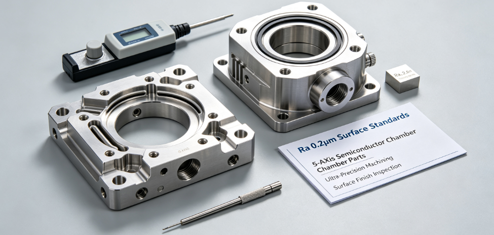
What Exactly Is Ra 0.2 μm for Semiconductor Chamber Parts?
First, a quick refresher:
Ra (Arithmetic Mean Roughness) measures average height deviation of peaks and valleys on a machined surface. Lower Ra = smoother surface.
Ra 0.2 μm = 0.2 micrometers average roughness.
For semiconductor vacuum applications, this spec carries strict unwritten rules most general machine shops ignore:
- Measurement direction matters: readings must be taken across machining marks, not parallel to them.
- Sampling length and cutoff filters follow ISO 4287 standards for vacuum hardware.
- Ra 0.2 μm target is typically a maximum limit (Ra ≤ 0.2 μm), not nominal.
- Finish must be consistent on curved surfaces, internal corners, and deep cavity walls — not just flat external faces.
This is not a general-purpose polished finish. Semiconductor chamber surfaces require low surface area to minimize:
- Adsorption of water vapor, hydrocarbons and process residuals
- Particle generation during thermal cycling, plasma exposure and maintenance
- Slow pump-down and unstable ultra-high vacuum (UHV) pressure
Rough surfaces act like tiny sponges. Every microscopic valley holds contaminants that slowly release into your process chamber. Even small shifts in background pressure can create non-uniform wafer processing and drag down yield.
Why Semiconductor OEMs Standardize on Ra 0.2 μm for Critical Chamber Surfaces
Let’s cut through theory with real fab pain points:
1. Lower outgassing rates
Smoothed surfaces reduce available surface area where gas molecules stick. Compared to Ra 0.8 μm or Ra 1.6 μm machined surfaces, Ra 0.2 μm significantly reduces trapped volatiles. This shortens required bakeout cycles and helps you reach stable UHV faster.
2. Reduced particle shedding
Sharp tool peaks break off under thermal stress or plasma bombardment. Ra 0.2 μm eliminates jagged micro-edges that become contamination sources inside the process volume. For advanced node fabs, stray particles directly translate to wafer defects.
3. Better seal integrity on vacuum flanges
Gaskets and metal seals rely on consistent surface texture. Too rough, and seals leak; overly polished surfaces can risk stick-slip. Ra 0.2 μm hits the sweet spot for many copper, aluminum and fluoropolymer vacuum sealing interfaces.
4. Stable plasma performance
Many etch and deposition chambers run continuous plasma. Uneven rough surfaces trigger localized field emission, inconsistent plasma density and unwanted arcing. Uniform Ra 0.2 μm surfaces support predictable, repeatable process conditions batch after batch.
Why 5-Axis Machining Is Non-Negotiable for Consistent Ra 0.2 μm Results
You can polish simple flat plates to Ra 0.2 μm on a 3-axis machine. Complex semiconductor chamber bodies? That’s a different challenge.
Semiconductor chambers feature:
- Deep enclosed cavities
- Compound-angle gas ports
- Undercut geometry
- Mixed curved and planar surfaces
- Tight internal radii with limited tool access
Here’s how 5-axis changes the game:
Single-setup machining
No repeated re-clamping. Eliminates alignment shifts that create uneven surface quality across separate operations.
Optimized tool vector control
The machine tilts spindles to keep cutting tools normal or near-normal to complex surfaces. Minimal tool deflection = fewer chatter marks — the biggest enemy of tight Ra specs.
Continuous finishing passes over freeform geometry
3-axis machines often force long, slender tools into awkward angles, causing vibration and streaky surface texture. 5-axis shortens required tool length and improves rigidity.
Uniform finish inside deep pockets & corners
Internal radii and chamber walls often fail roughness checks when machined on 3-axis equipment. 5-axis reaches hard-to-access zones without sacrificing surface quality.
Important note:
5-axis machining alone rarely hits Ra 0.2 μm straight off the cutter. Most material combinations (6061 aluminum, 316L stainless) require a carefully sequenced workflow:
- Roughing
- Semi-finish 5-axis milling
- Precision finishing passes with small-radius end mills
- Controlled mechanical finishing or electropolishing (application dependent)
- Full surface roughness verification with profilometry
Material-Specific Notes for Ra 0.2 μm Semiconductor Chamber Hardware
Different common chamber metals behave differently when targeting Ra ≤ 0.2 μm:
- 6061 / 7075 Aluminum: Very machinable via 5-axis. Typically requires light post-machining finishing. Must follow proper passivation and cleanroom cleaning to avoid oxidation. Widely used for transfer chambers, load locks and manifolds.
- 316L Stainless Steel: Harder to machine. Prone to built-up edge on cutting tools. Consistent Ra 0.2 μm often requires electropolishing after 5-axis machining. Ideal for high-temperature UHV and corrosive process environments.
- Copper & Copper Alloys: Excellent thermal conductivity for chucks and cooling components. Soft material demands sharp tooling and low chip loads to avoid tearing surface grain.
Over-spec warning:
Ra 0.1 μm or mirror finishes sound appealing, but they add major cost and longer lead times. For most non-optical chamber surfaces, Ra 0.2 μm delivers the performance balance semiconductor equipment teams need without unnecessary manufacturing overhead.
Real-World Challenge: Common Mistakes When Specifying Ra 0.2 μm
- Writing “Ra 0.2 μm maximum” without defining measurement standard (ISO 4287 is mandatory for vacuum parts).
- Applying Ra 0.2 μm to non-critical external surfaces, inflating component cost.
- Expecting uniform Ra 0.2 μm without accounting for tight internal radii geometry.
- Choosing vendors without dedicated cleanroom finishing and profilometry validation.
- Separating machining and finishing operations across multiple suppliers, introducing handling contamination.
FAQ
Can we achieve Ra 0.2 μm directly from 5-axis milling without secondary polishing?
It depends heavily on material and geometry. On flat, open aluminum surfaces with rigid fixturing, premium high-speed 5-axis centers can hit near Ra 0.2 μm. For deep cavities, stainless steel, tight internal radii and curved surfaces, secondary controlled finishing or electropolishing is almost always required to guarantee consistent Ra ≤ 0.2 μm across all features. Never rely on as-milled surface finish for semiconductor UHV critical surfaces.
What’s the difference between Ra 0.2 μm and Ra 0.4 μm for vacuum chamber performance?
Ra 0.4 μm is widely used for less critical vacuum hardware. Ra 0.2 μm delivers noticeably lower effective surface area, slower outgassing rates, fewer particle emission risks and more stable plasma behavior. For advanced-node etch, ALD and PVD chambers where yield sensitivity is high, engineering teams increasingly shift critical internal surfaces to Ra 0.2 μm.
Does Ra 0.2 μm replace electropolishing requirements for stainless steel UHV chambers?
No. Electropolishing modifies the metal grain structure and creates a passive chromium oxide layer, which delivers long-term low outgassing benefits you cannot achieve via mechanical finishing alone. You can target Ra 0.2 μm as the final surface target after electropolishing, but roughness spec and surface treatment are separate requirements.
Will Ra 0.2 μm surfaces hold up under repeated thermal bakeout and plasma cycling?
Yes — when properly finished and cleaned. The main risk is residual machining debris trapped in micro-valleys. That’s why controlled finishing and rigorous cleanroom cleaning protocols are mandatory alongside the roughness spec. Poorly cleaned Ra 0.2 μm surfaces perform worse than well-cleaned Ra 0.4 μm surfaces.
Can 5-axis machining guarantee identical Ra 0.2 μm results on prototypes and production runs?
Only if the vendor locks in tool paths, cutting parameters, tool grades, fixturing strategy and environmental temperature stability. Semiconductor-grade manufacturers maintain documented machining workflows and sample profilometry audits to avoid drift between prototype and volume batches. Ask suppliers for surface roughness capability reports (Cp/Cpk data).
Should I specify Ra 0.2 μm on every surface of my chamber component?
Not recommended. Use surface finish zoning in your drawings. Label internal process-wetted surfaces as Ra ≤ 0.2 μm, and assign relaxed Ra values to mounting bosses, external brackets or non-vacuum surfaces. This controls manufacturing cost without compromising process performance.
How do I verify that delivered parts truly meet Ra 0.2 μm spec?
Require contact profilometry reports following ISO 4287. Random sampling on curved surfaces, corners and deep cavities — not just easy-to-reach flat areas. Avoid relying solely on visual inspection; human eyes cannot reliably distinguish Ra 0.2 μm vs Ra 0.4 μm.
Closing Thoughts
Surface roughness is not just a line item on your drawing. Ra 0.2 μm is a performance specification that directly impacts vacuum stability, particle levels, bakeout time and wafer yield.
5-axis CNC machining is the foundation for achieving this standard on the complex multi-surface geometry typical of modern semiconductor vacuum chambers. But consistent results rely on more than just advanced machine tools: controlled finishing, material expertise, cleanroom handling and rigorous metrology all need to be built into the manufacturing workflow.
If you’re designing next-generation chamber hardware, start early conversations with your machining partner about surface zoning, measurement standards and manufacturability of your Ra requirements. Small adjustments at the design stage often deliver big savings in lead time and component cost.