Published:Zorapid.Ltd
If you’re machining semiconductor fixtures, jigs, wafer chucks, or handling plates, you already know one hard truth: standard CNC milling settings won’t cut it.
Semiconductor tooling requires ultra-tight tolerances, particle-free surfaces, minimal burrs, and low thermal deformation. Bad high-speed milling (HSM) parameters create micro-cracks, built-up edge, vibration-induced chatter, and loose debris — and that debris ruins expensive wafers and pollutes cleanroom workflows.
High-speed milling isn’t just spin the tool faster. It’s a balanced combo of spindle RPM, feed per tooth, depth of cut, tool selection, and cooling. Mess up one variable, and your fixture fails fab qualification.
Today we’re sharing workshop-tested HSM starting parameters for the most common semiconductor fixture materials, plus practical rules you can hand straight to your CNC programmers.
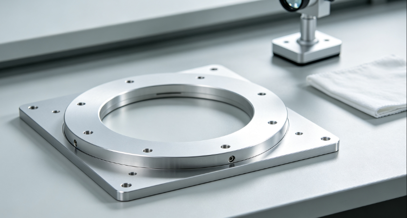
Why Semiconductor Fixture Milling Is Nothing Like Standard CNC Machining
Let’s cut straight to the point. Semiconductor fabrication environments are extremely unforgiving. A minor machining defect that’s acceptable for regular mechanical parts will cause huge losses in wafer processing. Here’s what makes semiconductor fixture HSM unique and challenging:
- Zero particle tolerance: Even micro-burrs or tiny chip residues can detach in cleanrooms, scratch wafer surfaces, and contaminate production lines.
- Micron-level tight tolerances: Most wafer contact fixtures require ±0.001mm positional tolerance and ultra-flat parallelism, leaving no room for thermal warpage or tool vibration errors.
- Thin-walled & delicate geometries: Many vacuum fixtures and wafer holders feature thin support walls and hollow structures that flex easily under heavy cutting forces.
- Low-outgassing & cleanroom compliance: Residual stress, surface roughness, and machining residues directly affect vacuum performance and cleanroom qualification.
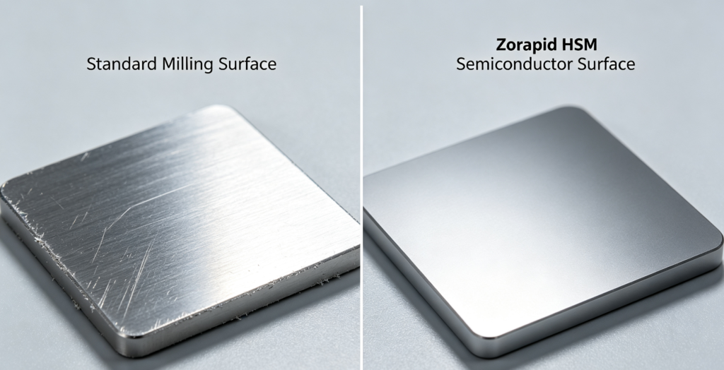
- No post-polishing allowed: Manual polishing introduces embedded particles and alters precision dimensions. All perfect finishes must be achieved via pure HSM finishing passes.
Traditional milling uses heavy depth cuts and aggressive radial engagement to save cycle time. For semiconductors, this creates excessive heat, residual stress, and micro-defects. Professional semiconductor HSM relies on fast spindle speed, light cuts, stable chip evacuation, and low-force toolpaths.
Complete HSM Parameter Cheat Sheet for Semiconductor Fixtures (2026 Updated)
Below are our production-validated baseline parameters for the top 5 semiconductor fixture materials. These settings are optimized for G2.5 balanced carbide end mills, high-rigidity HSM CNC machines, and cleanroom-grade tooling requirements. All values are safe starting points — adjust ±10% based on your machine condition, tool overhang, and part geometry.
Universal Rule for All Semiconductor Fixtures: Always use climb milling for finishing passes.
| Fixture Material | Typical Semiconductor Application | Roughing HSM Parameters | Finishing HSM Parameters | Critical Machining Tips |
|---|---|---|---|---|
| 6061-T6 Aluminum | Wafer base plates, handling jigs, standard cleanroom fixtures | RPM: 16,000–24,000Fz: 0.05–0.08 mm/toothAe: 15–25% tool diameterAp: 0.3–0.6mm | RPM: 22,000–32,000Fz: 0.03–0.05 mmtoothAe: 5–12% tool diameterAp: 0.1–0.2mm | Use MQL air-oil mist; avoid flood coolant to prevent residue; prevent built-up edge with sharp uncoated tools |
| 7075-T6 Aluminum | High-load vacuum fixtures, precision clamping plates, structural tooling | RPM: 14,000–20,000Fz: 0.04–0.07 mmtoothAe: 12–20% tool diameterAp: 0.25–0.5mm | RPM: 18,000–28,000Fz: 0.025–0.04 mmtoothAe: 4–10% tool diameterAp: 0.08–0.15mm | Higher tensile strength causes easier BUE; strictly avoid tool dwell on finished surfaces; shorten tool overhang |
| 316L Stainless Steel | Gas distribution fixtures, corrosive-resistant cleanroom tooling, vacuum flanges | RPM: 5,000–8,000Fz: 0.02–0.03 mm/toothAe: 10–18% tool diameterAp: 0.15–0.3mm | RPM: 7,000–11,000Fz: 0.012–0.022 mmtoothAe: 3–8% tool diameterAp: 0.05–0.1mm | Severe work hardening risk; no idle tool rubbing; use high-pressure precise coolant; slow acceleration CAM settings |
| Ti-6Al-4V Titanium | Ultra-low-outgassing vacuum components, high-stability process fixtures | RPM: 6,000–10,000Fz: 0.02–0.04 mm/toothAe: 12–20% tool diameterAp: 0.2–0.4mm | RPM: 8,000–14,000Fz: 0.015–0.03 mm/toothAe: 4–9% tool diameterAp: 0.06–0.12mm | Poor thermal conductivity; strictly light cuts; focused coolant to avoid heat accumulation; prevent tool burn |
| ESD PEEK | Wafer grippers, insulating fixtures, anti-static cleanroom components | RPM: 8,000–15,000Fz: 0.04–0.07 mm/toothAe: 18–25% tool diameterAp: 0.3–0.5mm | RPM: 12,000–20,000Fz: 0.025–0.04 mmtoothAe: 6–12% tool diameterAp: 0.1–0.18mm | Dry air blast only; strictly control cutting heat to avoid melting and material deformation |
7 Non-Negotiable HSM Rules for Semiconductor Fixture Machining
Parameters are important, but process discipline is what makes fixtures pass cleanroom inspection. These 7 rules are what we follow at Zorapid for every semiconductor project — skip any of them, and you’ll face quality risks.
1. All Tool Assemblies Must Be G2.5 Balanced
At 20,000+ RPM, even tiny tool holder unbalance causes micro-vibration. Vibration creates subtle chatter marks, uneven surface roughness, and invisible micro-cracks on fixture surfaces. For semiconductor tooling, we balance every tool + holder assembly to G2.5 tolerance, no exceptions.
2. Minimize Tool Overhang to Eliminate Chatter
Long tool overhang is the #1 cause of unstable finishing. Always use the shortest tool possible to clear part geometry. Shorter tools deliver higher rigidity, consistent chip load, and perfectly uniform finish — critical for wafer contact surfaces.
3. Use Trochoidal Roughing Instead of Heavy Slotting
Heavy full-width slotting generates huge cutting force and residual stress. Trochoidal toolpaths maintain light radial engagement, reduce workpiece deformation, and extend tool life. It adds a little cycle time but completely eliminates warpage on thin-walled semiconductor fixtures.
4. Never Let Tools Dwell on Finished Surfaces
Tool dwell creates tiny indentations and thermal marks. These subtle defects don’t show up in basic dimension checks but will shed micro-particles in cleanroom operation. Always program continuous tool movement on all critical finishing areas.
5. Optimize Chip Evacuation 100%
Trapped chips scratch mirror-finish surfaces and create local hot spots. For aluminum fixtures, use filtered MQL mist; for plastic parts, use clean dry air blast. Zero trapped chips = zero surface contamination.
6. Strictly Separate Roughing & Finishing Operations
Roughing leaves stress on the workpiece. We always release residual stress before finishing cuts, ensuring final dimensions stay stable in cleanroom temperature and humidity environments.
7. Post-Machining Precision Cleaning Is Mandatory
Ordinary air blowing is not enough. All Zorapid semiconductor fixtures go through ultrasonic cleaning, dust-free wiping, and sealed packaging to guarantee cleanroom compatibility.
What Makes Zorapid Different From Ordinary CNC Shops? (Core Advantages for Semiconductor Clients)
Many machining shops can run high-speed milling. But very few understand semiconductor cleanroom standards, particle control, and low-outgassing requirements. Zorapid specializes in semiconductor precision tooling, with process systems built exclusively for fab-grade quality.
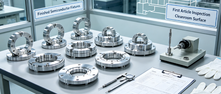
1. Validated Semiconductor HSM Parameter Library
We don’t rely on generic CNC settings. We have a fully tested, project-validated HSM parameter database for all mainstream semiconductor fixture materials (6061, 7075, 316L, Titanium, ESD PEEK). Every parameter is verified by real cleanroom fixture projects, eliminating trial-and-error scrap and unstable quality.
2. Micron-Level Repeatable Precision
Our dedicated HSM precision machining cells support consistent tolerance control down to ±0.001mm. Every finished fixture undergoes full dimensional inspection, flatness testing, and surface roughness detection. We guarantee 100% dimensional consistency for prototype and mass orders.
3. Full Particle & Contamination Control Workflow
We optimize toolpaths to minimize burr generation fundamentally, instead of relying on post-processing repair. Our standardized post-machining process includes precision deburring, ultrasonic cleaning, dust-free inspection, and vacuum-sealed packaging. This strict workflow ensures every fixture is cleanroom-ready and zero-contamination.
4. Full Material Traceability & Low-Outgassing Compliance
All raw materials we use come with complete material certificates, batch reports, and low-outgassing test data. We strictly select semiconductor-grade raw materials to avoid outgassing, oxidation, and vacuum performance degradation, fully meeting EU and US semiconductor fab standards.
5. Fast Prototype to Mass Production Consistency
Whether you need one-off R&D prototypes or small-batch mass production, we lock fixed HSM parameters, tool standards, and process flows. Every batch of fixtures maintains identical precision and surface quality, avoiding the common problem of “prototype good, mass production unstable”.
6. Professional DFMA Design Optimization Support
Our engineering team provides free design optimization during quoting. We tweak fixture geometry, wall thickness, and machining allowance to reduce HSM vibration, eliminate machining risks, lower production costs, and improve the long-term stability of your fixtures in fab operation.
7. Strict Quality Control & Full Inspection Reports
We deliver full inspection data with every order: dimension reports, Ra surface roughness data, flatness records, and material certification. Perfect for your internal quality audit and customer compliance review.
FAQ
Can I use standard HSM parameters for thin-walled semiconductor fixtures?
Absolutely not. Thin-walled structures are extremely flexible. Standard parameters will cause bending, warpage, and chatter. We recommend reducing feed per tooth by 15–25%, lowering radial engagement, slowing CAM acceleration/deceleration, and adding auxiliary support during machining. Always use customized light-cut parameters for thin-wall fixture finishing.
What is the ideal surface roughness for wafer contact fixture surfaces?
Ra ≤ 0.4μm is the universal standard for most US/EU semiconductor wafer contact surfaces. We achieve this purely via optimized HSM finishing passes. Manual polishing is forbidden because it introduces embedded particles and breaks precision flatness.
Is flood coolant acceptable for semiconductor fixture machining?
Depends on your application scenario. Flood coolant extends tool life but leaves micro-residues. For non-cleanroom structural fixtures, it’s fine. For wafer contact, vacuum, and cleanroom critical parts, we use MQL mist or dry air machining, followed by professional ultrasonic cleaning to ensure zero residue.
How to completely eliminate built-up edge (BUE) on aluminum fixtures?
BUE is the top enemy of aluminum semiconductor fixtures. Solve it with 3 key steps: 1) Use sharp, polished 2–3 flute uncoated carbide tools; 2) Avoid ultra-light feed rates that cause tool rubbing; 3) Stabilize spindle speed and MQL lubrication. Replace worn tools immediately — dull tools are the main cause of BUE.
What is the most costly HSM mistake in semiconductor fixture manufacturing?
Overly aggressive radial cuts to save cycle time. Many shops prioritize efficiency and use large Ae cutting, which generates massive residual stress, micro-burrs, and invisible warpage. These defects won’t show up immediately but will cause fixture deformation and particle shedding during long-term cleanroom use. Light, stable cuts always beat fast, risky cuts for semiconductor tooling.
Can Zorapid customize HSM parameters for our in-house machines?
Yes, fully customizable. Share your machine’s maximum RPM, tool holder type, machine rigidity, and target tolerance requirements. Our engineering team will adjust our baseline HSM parameters to match your equipment, helping you replicate fab-grade machining quality in your own workshop. We also provide full-turnkey fixture manufacturing services.
How do you guarantee zero-particle performance for cleanroom fixtures?
It’s a full-process guarantee. We control particle sources from toolpath design, cutting parameters, tool selection, post-deburring, ultrasonic cleaning, to dust-free sealed packaging. Every fixture is inspected for micro-residues before delivery, fully compliant with US and EU cleanroom semiconductor standards.
Final Thoughts
High-speed milling for semiconductor fixtures is never just a simple machining process. It’s a precise combination of parameter optimization, process control, quality management, and cleanroom compliance. Small parameter mistakes lead to huge fab yield losses, while standardized, validated HSM processes deliver stable, long-lasting, contamination-free fixture performance.
If you’re tired of unstable fixture quality, frequent scrap, and cleanroom validation failures, Zorapid’s semiconductor-focused HSM machining service is your reliable solution. We turn your CAD designs into fab-qualified, particle-free, high-precision semiconductor fixtures that meet strict US and EU manufacturing standards.
Send your drawings today for a customized quote and professional HSM process consultation!